Buletin Ilmiah Sarjana Teknik Elektro ISSN: 2685-9572
High Accuracy Dual Probe Station for Near Field Scanning
Tito Yuwono 1, Mohd Hafiz Baharuddin 2
1 Department of Electrical Engineering, Islamic University of Indonesia
2 Department of Electrical, Electronic, and System Engineering, Universiti Kebangsaan Malaysia, Malaysia
ARTICLE INFORMATION |
| ABSTRACT |
Article History: Submitted 11 September 2023 Revised 29 October 2023 Accepted 07 November 2023 |
| 
Electromagnetic (EM) emissions are a major issue for electronic products. Besides electronic products being able to work according to their function, they must also comply with EMC standards to avoid producing excessive EM emissions. One technique for measuring EM emissions is near field measurements. This measurement technique can be used to determine the faulty components which contribute to the failure of complying to the EMC standards. A near field measurement system consists of near field probes, digital oscilloscope, and a probe station which can control the movement of the near field probe during measurement process. In this paper, the design and development of a dual probe near field measurement system or station with high accuracy will be discussed. From instrument testing, it can be concluded that the probe station can cover ample scanning area with movement accuracy up to 0.05 mm and it is able to work well according to the test scenario. The designed probe station is verified by measurement and highly recommended to be used for near field measurements. |
Keywords: Near Field; Instrument; Dual Probe; Three Axis; High Accuracy |
Corresponding Author: Tito Yuwono, Department of Electrical Engineering, Islamic University of Indonesia, Yogyakarta, Indonesia. Email: tito@uii.ac.id |
This work is licensed under a Creative Commons Attribution-Share Alike 4.0 
|
Document Citation: T. Yuwono and M. H. Baharuddin, “High Accuracy Dual Probe Station for Near Field Scanning,” Buletin Ilmiah Sarjana Teknik Elektro, vol. 5, no. 4, pp. 417-426, 2023, DOI: 10.12928/biste.v5i4.9132. |
- INTRODUCTION
Electromagnetic (EM) emissions, whether intentional or unintentional is produced by electronic products during its normal operation. Besides the electronic products being able to work according to their function, they must also comply with EMC standards which means they are not producing excessive EM emissions which could harm other electronic devices. Several EM emission measurement methods used include open area test site (OATS) [1]–[3], anechoic chamber [4]–[6], reverberation chamber [7]–[9], transverse electromagnetic (TEM) cell [10]–[12], compact antenna test range (CATR) [13]–[16] and near field scanning (NFS) can be used to measure the EM emissions [17]–[23]. Near field measurements of electronic products are one of the techniques for obtaining EM emission data from these products. Based on [24], near field measurement has significant advantages compared to other techniques. The near field measurement is not affected by interference or noise, relatively low cost and is capable of pointing out which components are faulty. In general, the EM emission standards produced by electronic products are shown in Figure 1 and Figure 2 [24]. The FCC divides electronic devices into two classes; Class A and Class B. Class A is for electronic devices for industrial, scientific and medical applications, while Class B is for electronic device applications in residential environments. In general, class B standards are stricter than class A. Figure 1 shows the release limits for class A and class B according to the FCC [25]. Emission standards based on CISPR (CISPR 22) are also divided into Class A and Class B. Figure 2 shows the maximum emission limits for class A and class B according to CISPR 22 (CISRP 2006). In CISPR 22, the measurement distance between the DUT and the receiving antenna is always 10 meters for both Class A and Class B. While in the FCC, the distance between the DUT and the receiving antenna is 10 meters for class A and 3 meters for class B [26].
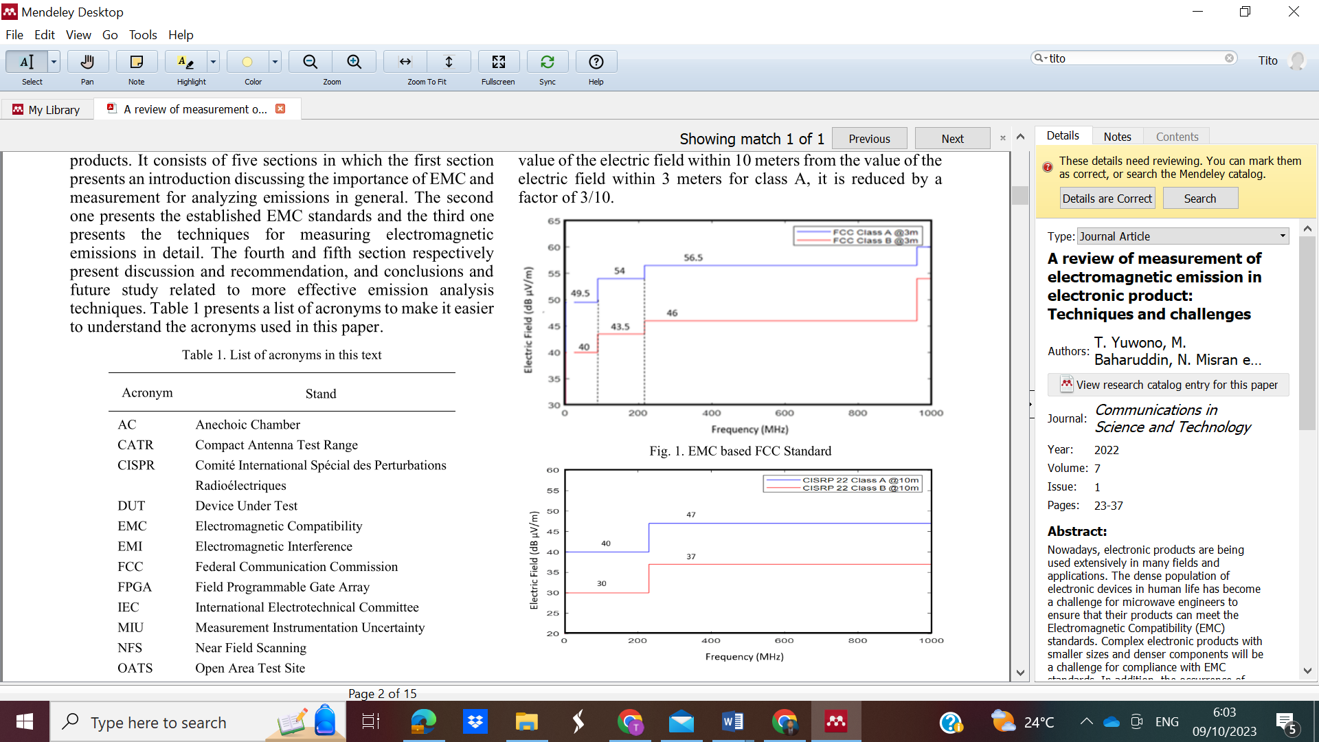
Figure 1. EMC Standard by FCC [24]
Figure 2. EMC Standard by CISRP [24]
One of the most important instruments in the near-field scanning system is the probe controller. During the near field measurement, the probe has to be moved to multiple points on a plane above the electronic device to measure the radiated emissions In order to get precise and accurate results from the scanning, the movement of the probe needs to be automated. Several probe controller instruments have been developed by researchers and companies where 1-probe controller instrument products have been produced [27]–[30] while the 2-probe controller device has also been studied by Stadtler et al [31] and Balmer [32].
The disadvantage of a 1-probe controller instrument is that it cannot perform correlation operations between scanning points. Correlation measurement is possible if scanning is carried out using 2 probes and the data is taken and stored at the same time. A high resolution and good accuracy of this operating machine will be the key to the near field characterization of the device under test. An automatic and high-resolution 2-probe actuation station is required to support more accurate emission measurements. This paper will present the design and development of an instrument to control the movement of 2 magnetic probes. The probe station is also capable of moving in 3 axis.
- METHODS
Performing the near field scanning requires the probes to be moved automatically with high accuracy and precision. Figure 3 illustrates a near field scanning system with two probes positioned above an electronic device (Device Under Test, DUT). The probe is moved according to a certain pattern to get the reading across the scanning plane. Measurements using two probes are required to calculate the correlation function from the measurements.
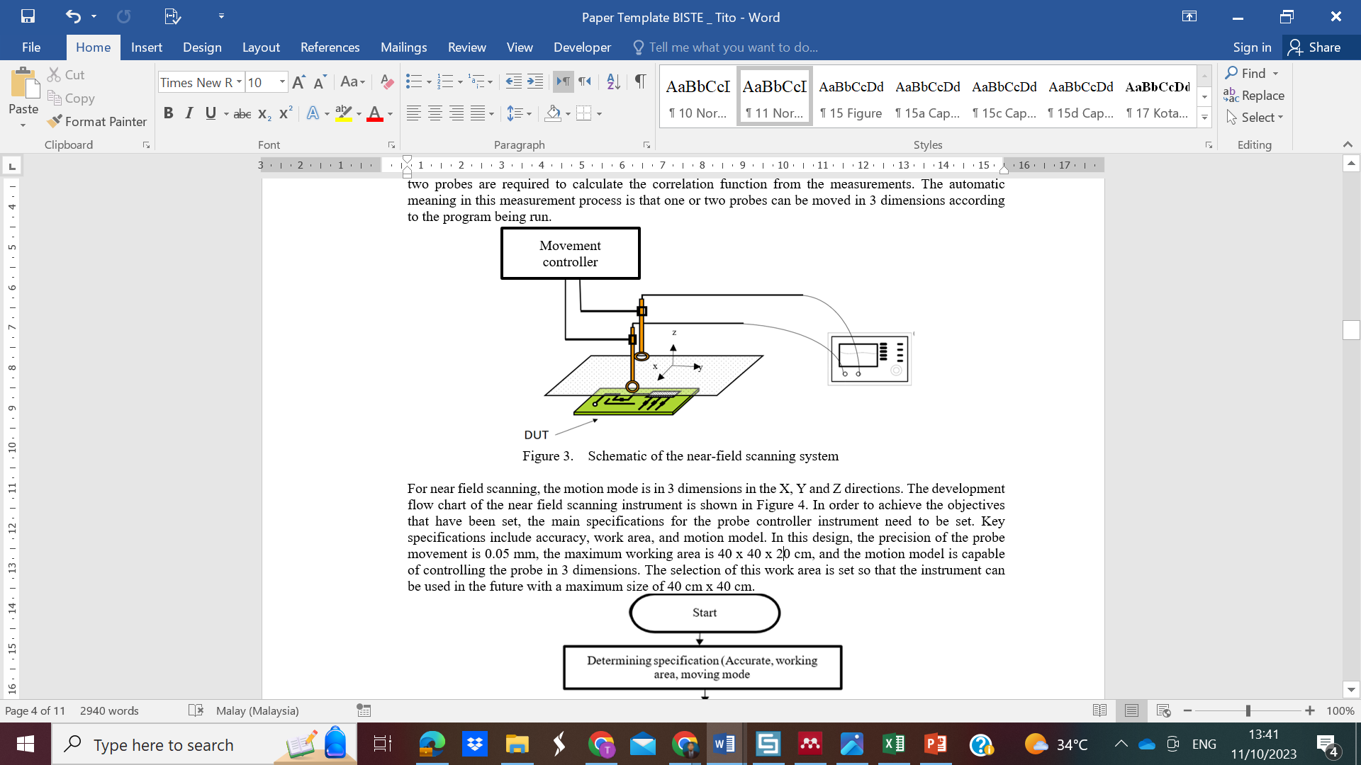
Figure 3. Schematic of the near-field scanning system
The motion mode for near field scanning will allow the probe to scan along 3 axes (X, Y and Z directions). The flow chart of the near field scanning instrument development is shown in Figure 4. In order to achieve the objectives, the main specifications for the probe controller instrument need to be determined. Key specifications include accuracy, work area, and motion model. In this design, the accuracy of the probe movement is 0.05 mm, the maximum working area is 40 x 40 x 20 cm, and the motion mode is capable of controlling the probe in 3 dimensions.
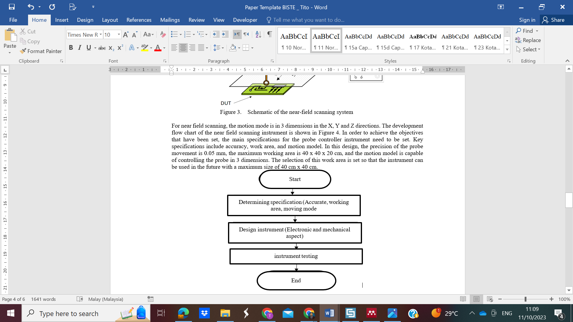
Figure 4. Flowchart of the steps for the development of a near-field scanning instrument
After determining the specifications of the instrument, we need to determine the mechanical and electrical components. The final step of this development is the testing and validation of the instrument. The aim of testing is to ensure that the instrument meets the specifications before it is ready to be used. For this test, we use Repetier software with the output G Code as shown in Figure 5.
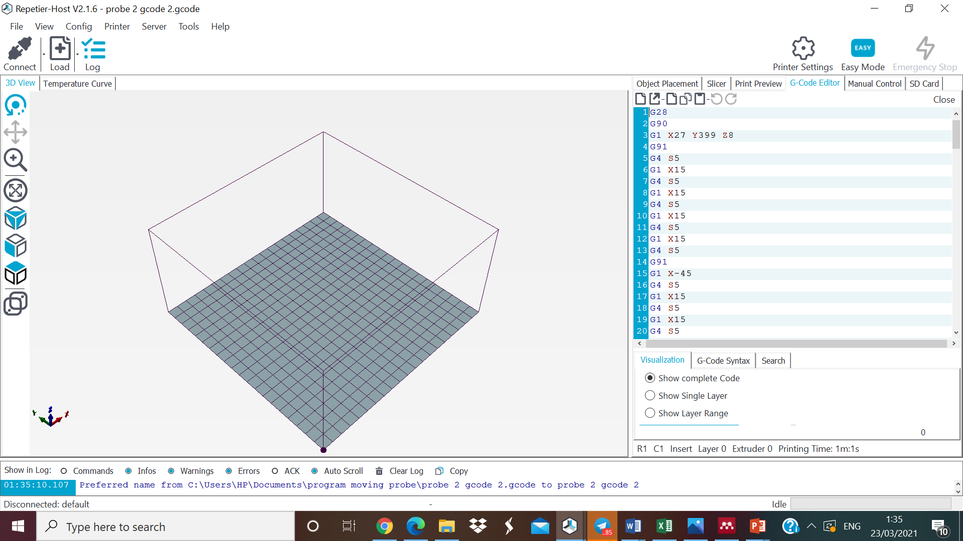
Figure 5. Repetier software display
- RESULT AND DISCUSSION
An automatic near field measurement instrument was developed with total dimensions of length 77 cm, width 67 cm and height 40 cm. This total dimension gives a working area of 40 x 40 x 20 cm. The frame material used is extruded aluminium 2020 and 2040. Figure 6 shows the instrument that has been built.
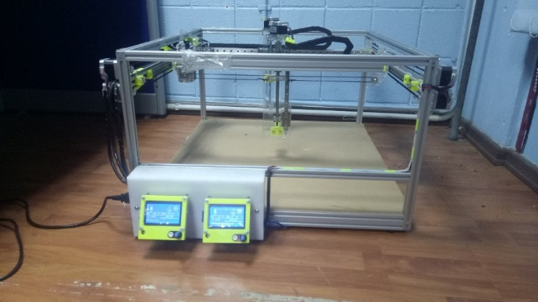
Figure 6. The result of the design of an automatic near-field measuring device
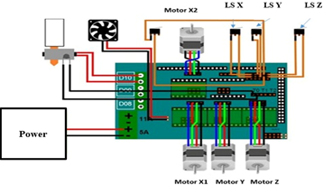
The entire actuation mechanism is combined with a rail of type MGN 12 C to produce a stable and smooth movement. The bracket to hold the actuator component is made of acrylic with a thickness of 8 mm. Some other components made of acrylic are the X-axis holder bracket, Y-axis holder bracket, Z-axis holder bracket, stepper motor bracket, probe holder bracket and control box. In addition, some components are made using a 3D printer machine such as the probe holder and cable bracket. This instrument controller is a combination of Ramps 1.4. Figure 7 shows the Ramps network. Ramps 1.4 works to simplify the control process where it can be used in a plug-and-play manner. Figure 8 shows the interconnection between components.
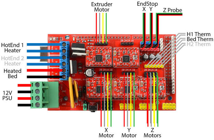
Figure 7. Ramps 1.4
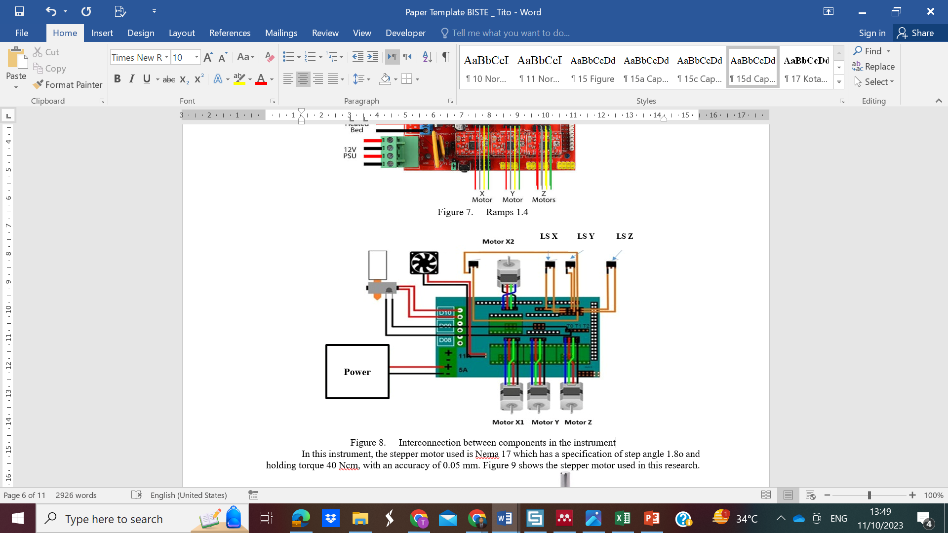
Figure 8. Interconnection between components in the instrument
In this instrument, the stepper motor used is Nema 17 which has a specification of step angle 1.8o and holding torque of 40 Nm, with an accuracy of 0.05 mm. Figure 9 shows the stepper motor used in this research. The DRV8825 driver is used to control the rotation of the stepper motor with a current setting at 1.3 A. This instrument uses two independent controller boards where each controller is programmed to control three stepper motors. The motor movement setting is done through the controller's LCD with a 128x64 dot matrix type. Figure 10 shows the instrument motion control board.
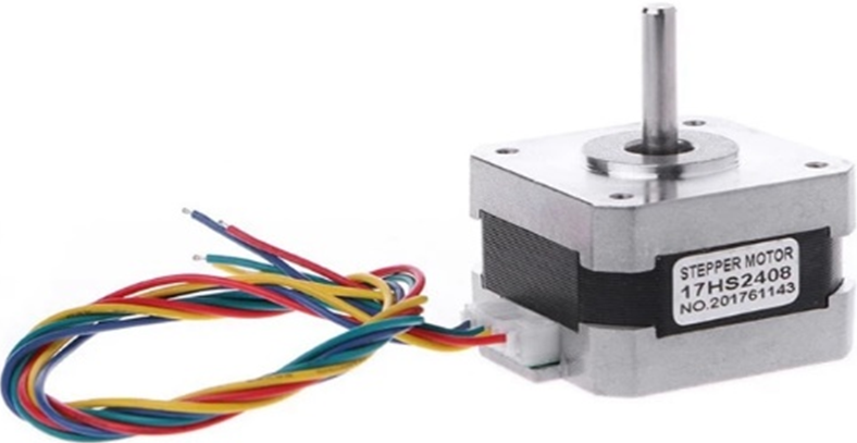
Figure 9. Stepper motor in the instrument
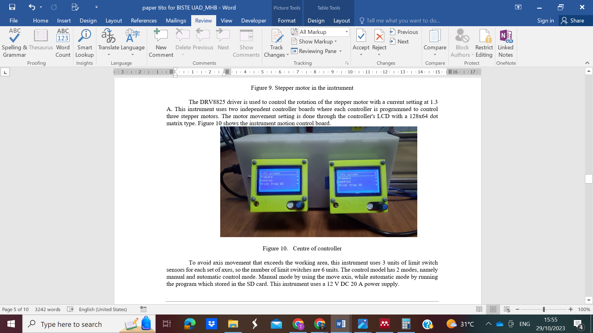
Figure 10. Centre of controller
To avoid axis movement that exceeds the working area, this instrument uses 3 units of limit switch sensors for each set of axes, so the number of limit switches are 6 units. The control model has 2 modes, namely manual and automatic control mode. Manual mode by using the move axis, while automatic mode by running the program which stored in the SD card. This instrument uses a 12 V DC 20 A power supply.
The performance of the instrument is measured based on two parameters, namely the accuracy and the motion based on the scenario and the program being run. The instrument is designed to be accurate to 0.05 mm (50 μm). The testing of this instrument is done by designing a program to allow the probe to move 100 steps with a total displacement distance of 5 mm, as shown in Figure 11. The G code used to test accuracy is shown in Figure 12.
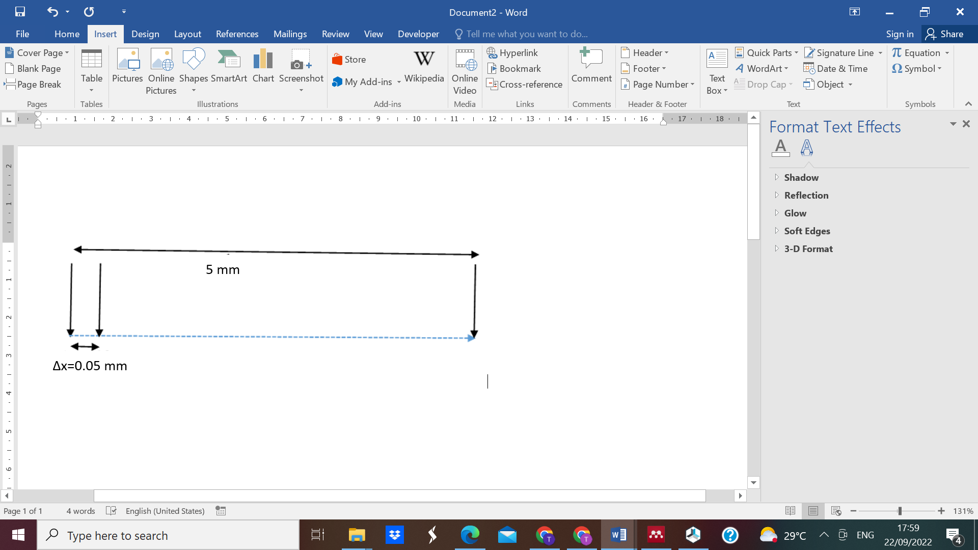
Figure 11. Accuracy testing
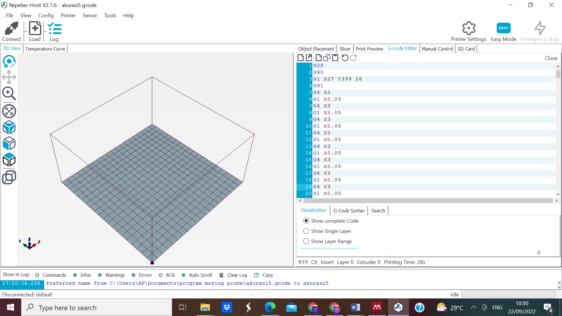
Figure 12. G code for accuracy testing
Probe movements were tested with two scenarios. First scenario, the movement follows the pattern as shown in Figure 13. Figure 14 shows the motion test for the first scenario. The second scenario is movement of two probes simultaneously as shown in Figure 15. Figure 16 shows the motion test for the second scenario
Figure 13. Probe movement for the first scenario
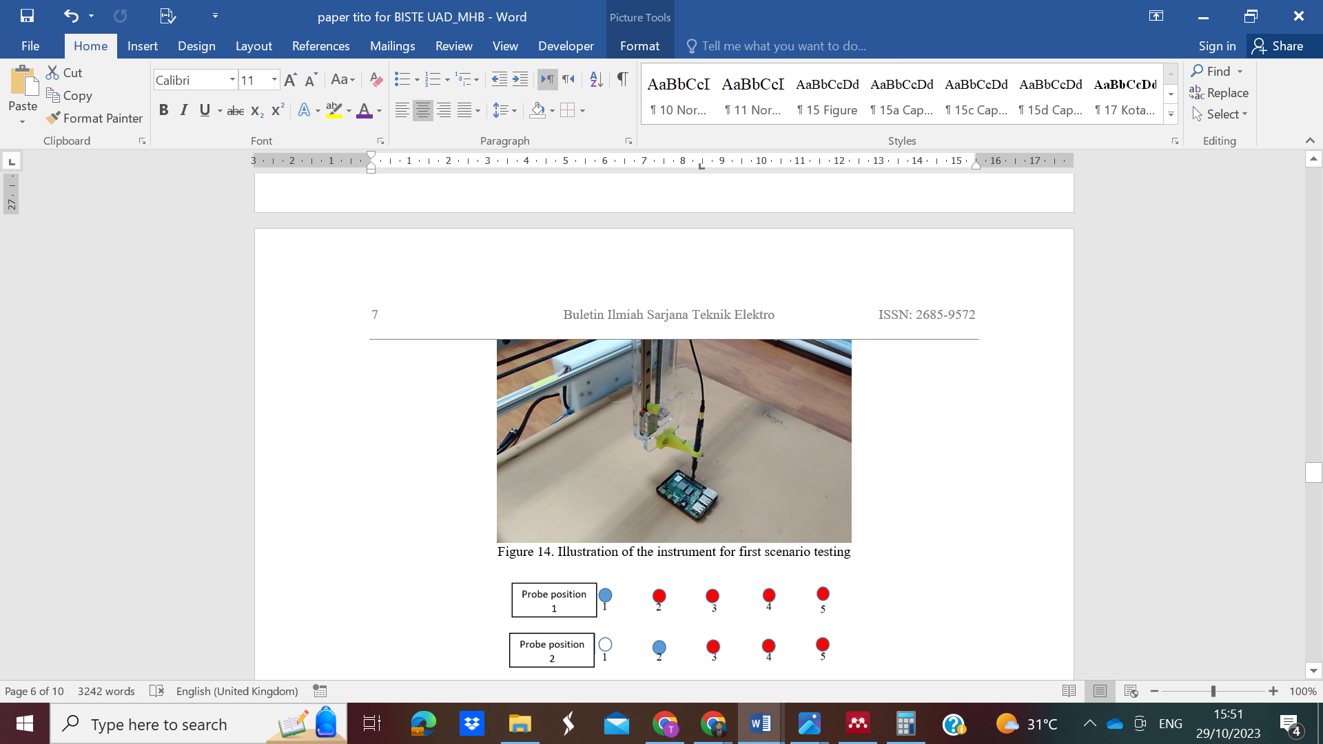
Figure 14. Illustration of the instrument for first scenario testing
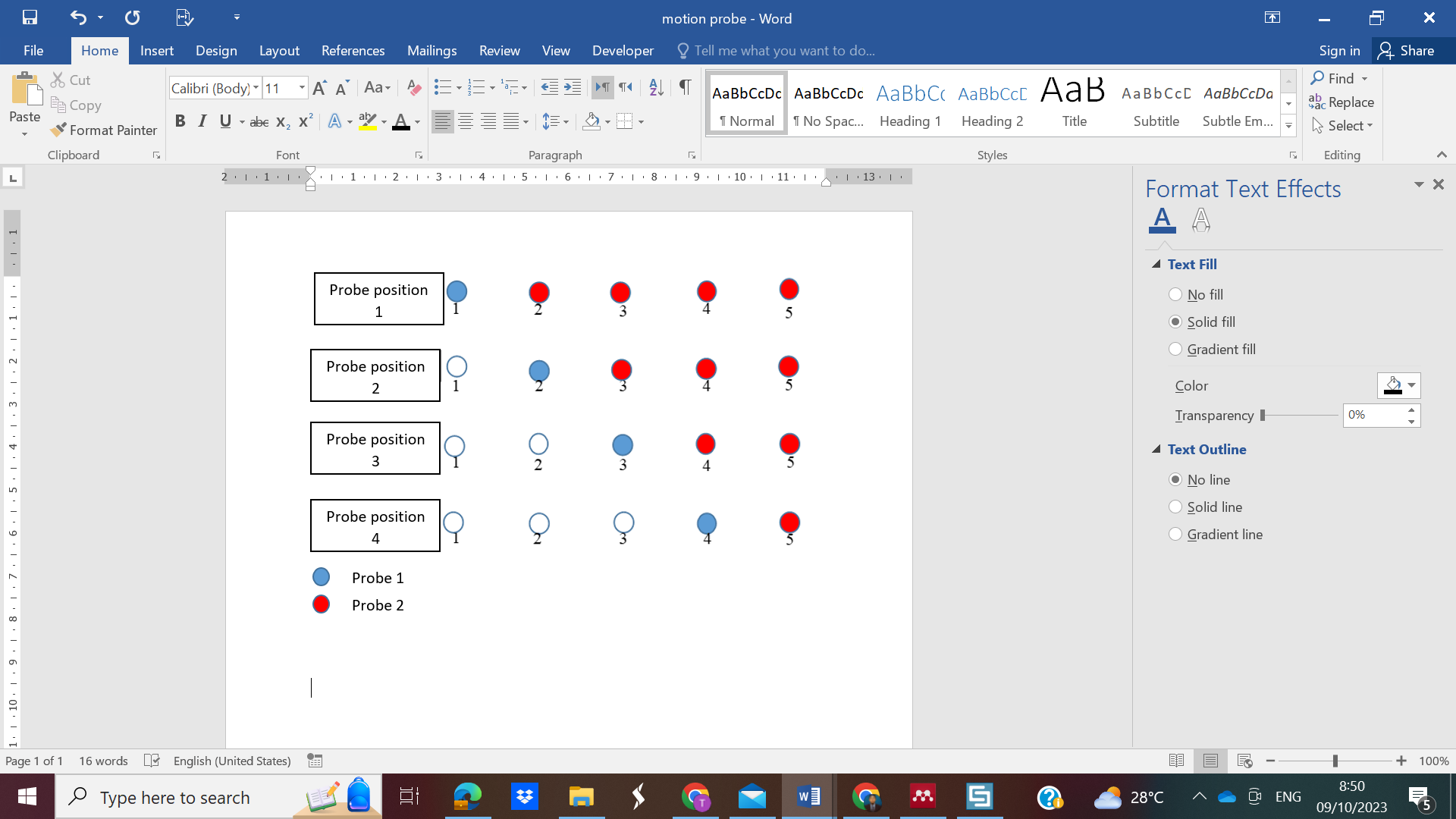
Figure 15. Testing movement of two probes simultaneously
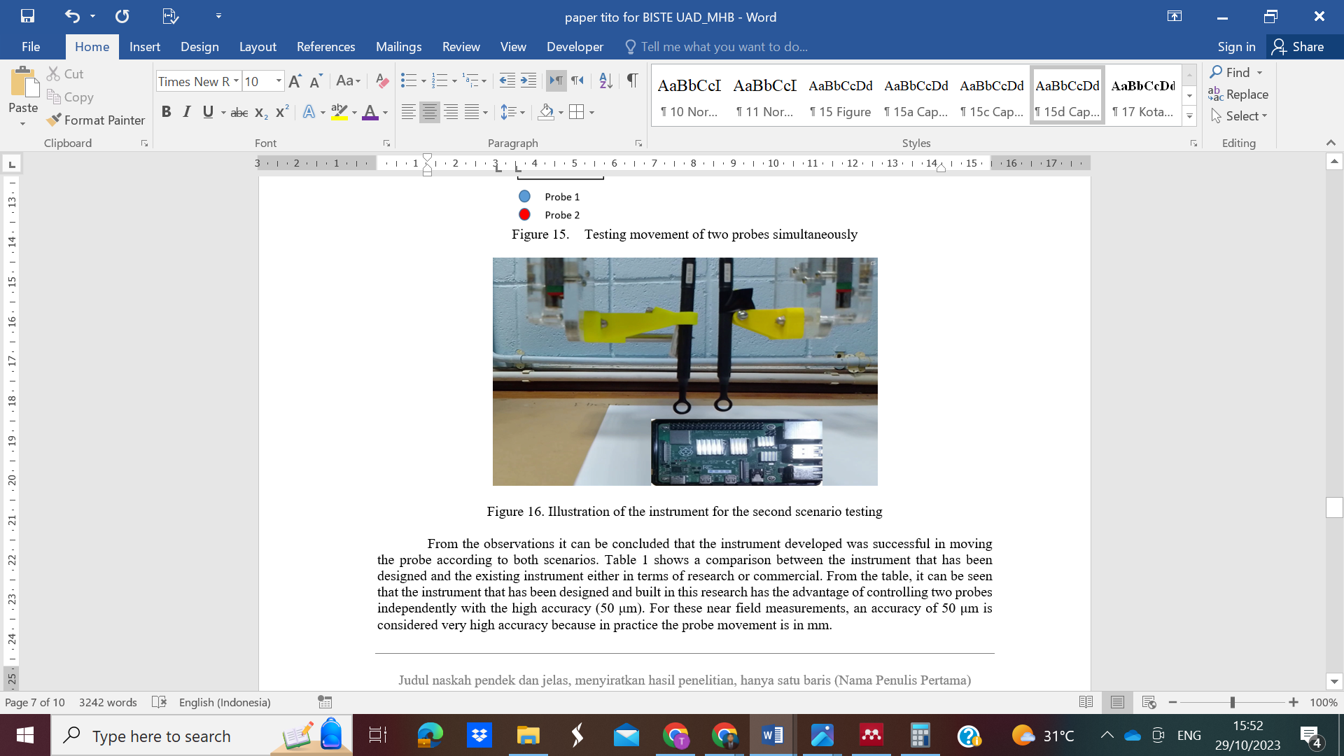
Figure 16. Illustration of the instrument for the second scenario testing
From the observations it can be concluded that the instrument developed was successful in moving the probe according to both scenarios. Table 1 shows a comparison between the instrument that has been designed and the existing instrument either in terms of research or commercial. From the table, it can be seen that the instrument that has been designed and built in this research has the advantage of controlling two probes independently with the high accuracy (50 μm). For these near field measurements, an accuracy of 50 μm is considered very high accuracy because in practice the probe movement is in mm.
Table 1. Comparison between instruments that have been designed and built with existing instruments
Reference | Number of probe | Accuracy |
[29] | 1 probe | 1μm |
[31] | 2 probe, 1 probe in the fix position | NAN |
[33] | 1 probe | 10μm |
[32] | 2 probe | NAN |
[30] | 1 probe | 10 μm |
[27] | 1 probe | 2μm |
[28] | 1 probe | NAN |
[34] | 1 probe | 50μm |
Instrument (Result of research) | 2 probe | 50 μm |
- CONCLUSIONS
The process of design, development and testing of instruments for near-field measurements has been described above. One of the important of the implementation of the near field scanning technique is the probe controller instrument. Existing probe controllers, both research and commercial products, are single-probe controllers. However, it cannot be used for cross-correlation operations between two measurement points. In this research, we developed an instrument for the measurement of EM emission which can move two probes simultaneously according to the scenario with high accuracy. The accuracy of the measurement distance is up to 50 μm. Maximum working area of this instrument are of 40 cm x 40 cm x 20 cm. With the above analysis, it is recommended that this instrument be used for near field measurements.
ACKNOWLEDGEMENT
The authors would like to acknowledge the financial support from the Directorate of Research and Community Services (DPPM), Islamic University of Indonesia and Geran Galakan Penyelidik Muda (GGPM) kod projek: GGPM-2020-005
REFERENCES
[1] F. G. Awan and A. Kiran, “Cancellation of Interference for Emission Measurement in Open Area Test Site,” Measurement, vol. 111, pp. 183–196, 2017, https://doi.org/10.1016/j.measurement.2017.07.037.
[2] K. M. G. Santos, M. S. Novo, G. Fontgalland, M. B. Perotoni, and C. L. Andrade, “Shielding effectiveness measurements of coaxial cable and connectors using compact open area test site,” J. Microwaves, Optoelectron. Electromagn. Appl., vol. 16, no. 4, pp. 997–1011, 2017, https://doi.org/10.1590/2179-10742017v16i41018.
[3] Donglin Meng, Xiao Liu and Dabo Li, "Research on unwanted reflections in an OATS for precise omni antenna measurement," 2015 IEEE 6th International Symposium on Microwave, Antenna, Propagation, and EMC Technologies (MAPE), pp. 245-249, 2015, https://doi.org/10.1109/MAPE.2015.7510308.
[4] Q. Xu and Y. Huang. Anechoic and Reverberation Chambers: Theory, Design, and Measurements. John Wiley & Sons. 2019. https://books.google.co.id/books?hl=id&lr=&id=eH9xDwAAQBAJ.
[5] K. Malaric, D. Muha, B. Saravanja, and T. Pusic, “Shielded Fabric Mini Anechoic Test Chamber,” in 2019 International Symposium ELMAR, pp. 81–84, 2019, https://doi.org/10.1109/ELMAR.2019.8918649.
[6] P. Kyösti, L. Hentilä, W. Fan, J. Lehtomäki and M. Latva-Aho, "On Radiated Performance Evaluation of Massive MIMO Devices in Multiprobe Anechoic Chamber OTA Setups," in IEEE Transactions on Antennas and Propagation, vol. 66, no. 10, pp. 5485-5497, 2018, https://doi.org/10.1109/TAP.2018.2860635.
[7] J. Zheng, X. Chen, X. Liu, M. Zhang, B. Liu, and Y. Huang, “An Improved Method for Reconstructing Antenna Radiation Pattern in a Loaded Reverberation Chamber,” IEEE Trans. Instrum. Meas., vol. 71, pp. 1–12, 2022, https://doi.org/10.1109/TIM.2022.3151937.
[8] A. Reis, F. Sarrazin, P. Besnier, P. Pouliguen, and E. Richalot, “Contactless Antenna Gain Pattern Estimation from Backscattering Coefficient Measurement Performed Within a Reverberation Chamber,” IEEE Trans. Antennas Propag., vol. 70, no. 3, pp. 2318–2321, 2022, https://doi.org/10.1109/TAP.2021.3111184.
[9] C. Carobbi and R. Serra, “Exponential correlation model for electric field intensity in reverberation chambers,” in 2022 16th European Conference on Antennas and Propagation (EuCAP), pp. 1–5, 2022, https://doi.org/10.23919/EuCAP53622.2022.9769629.
[10] M. Koohestani, M. Ramdani, P. Besnier, J. -L. Levant and R. Perdriau, "Perturbations of Electric and Magnetic Fields Due to the Presence of Materials in TEM Cells," in IEEE Transactions on Electromagnetic Compatibility, vol. 62, no. 4, pp. 997-1006, 2020, https://doi.org/10.1109/TEMC.2019.2928215.
[11] M. Koohestani, M. Ramdani, and R. Perdriau, “Impact of Mode Propagation on Radiated Immunity Characterization in Commonly Used TEM Cells,” in EMC COMPO 2019 - 2019 12th International Workshop on the Electromagnetic Compatibility of Integrated Circuits, pp. 5–7, 2019, https://doi.org/10.1109/EMCCompo.2019.8919742.
[12] M. Koohestani, M. Ramdani, P. Besnier, J. L. Levant, and R. Perdriau, “Perturbations of Electric and Magnetic Fields Due to the Presence of Materials in TEM Cells,” IEEE Trans. Electromagn. Compat., vol. 62, no. 4, pp. 997–1006, 2020, https://doi.org/10.1109/TEMC.2019.2928215.
[13] S. Pivnenko, A. U. Zaman, and M. Ivashina, “Using a Conical Horn as Compact Antenna Test Range Feed in Millimetre Bands,” in 2022 16th European Conference on Antennas and Propagation (EuCAP), pp. 01–05, 2022, https://doi.org/10.23919/EuCAP53622.2022.9769279.
[14] S. F. Gregson, M. Dirix, and R. Dubrovka, “Efficient Optimization of the Blended Rolled Edge of a Rectangular Single Offset-Fed Compact Antenna Test Range Reflector Using Genetic Evolution,” in 2022 16th European Conference on Antennas and Propagation (EuCAP), pp. 1–5, 2022, https://doi.org/10.23919/EuCAP53622.2022.9769585.
[15] J. Tang et al., “Compact Antenna Test Range Using Very Small F/D Transmitarray Based on Amplitude Modification and Phase Modulation,” IEEE Trans. Instrum. Meas., vol. 71, pp. 1–14, 2022, https://doi.org/10.1109/TIM.2022.3150835.
[16] Y. Chen, J. Yu, H. Ge, Y. Yao, and X. Chen, “Unified Initial Preprocessing for Phaseless Characterization of Quiet Zone in Millimeter-wave Compact Antenna Test Range,” IEEE Antennas Wirel. Propag. Lett., vol. 1225, pp. 1–1, 2022, https://doi.org/10.1109/LAWP.2022.3166757.
[17] P. Zuo, Y. Li, Y. Xu, H. Zheng, and E. P. Li, “Near-Field Radiation Estimation and Its Reduction Using a Novel EBG for PCB,” IEEE Trans. Components, Packag. Manuf. Technol., vol. 9, no. 2, pp. 329–335, 2019, https://doi.org/10.1109/TCPMT.2018.2829023.
[18] Q. Huang et al., “Radiation Emission Source Localization by Magnetic Near-Field Mapping Along the Surface of a Large-Scale IC with BGA Package,” IEEE Trans. Electromagn. Compat., vol. 64, no. 2, pp. 495–505, 2022, https://doi.org/10.1109/TEMC.2021.3123536.
[19] S. Pfennig, “Comparison of Three Methods for Testing IC’s to Field-Coupled Immunity and Emissions,” IEEE Lett. Electromagn. Compat. Pract. Appl., vol. 1, no. 2, pp. 37–43, 2022, https://doi.org/10.1109/LEMCPA.2019.2933157.
[20] J. Wang, Z. Yan, C. Fu, Z. Ma, and J. Liu, “Near-Field Precision Measurement System of High-Density Integrated Module,” IEEE Trans. Instrum. Meas., vol. 70, 2021, https://doi.org/10.1109/TIM.2021.3078000.
[21] W. Shao et al., “Design and Characterization of a Multi-Processed Differential Magnetic Field Probe by Using Asymmetric Calibration Method,” IEEE Sens. J., vol. 22, no. 6, pp. 5723–5731, 2022, https://doi.org/10.1109/JSEN.2022.3148002.
[22] A. Boyer, N. Nolhier, F. Caignet, and S. Ben Dhia, “On the Correlation Between Near-Field Scan Immunity and Radiated Immunity at Printed Circuit Board Level – Part I,” IEEE Trans. Electromagn. Compat., vol. 64, no. 4, pp. 1230–1242, 2022, https://doi.org/10.1109/TEMC.2022.3169183.
[23] X. Wu, F. Grassi, G. Spadacini, S. A. Pignari, U. Paoletti, and I. Hoda, “Test Design Methodology for Time-Domain Immunity Investigations Using Electric Near-Field Probes,” IEEE Trans. Electromagn. Compat., vol. 64, no. 3, pp. 603–612, 2022, https://doi.org/10.1109/TEMC.2022.3149537.
[24] T. Yuwono, M. H. Baharuddin, N. Misran, M. Ismail, and M. F. Mansor, “A review of measurement of electromagnetic emission in electronic product: Techniques and challenges,” Commun. Sci. Technol., vol. 7, no. 1, pp. 23–37, 2022, https://doi.org/10.21924/cst.7.1.2022.727.
[25] C. R. Paul, R. C. Scully, and M. A. Steffka. Introduction to electromagnetic compatibility. John Wiley & Sons. 2022. https://books.google.co.id/books?hl=id&lr=&id=A-eLEAAAQBAJ.
[26] H. Sekiguchi and S. Seto, "Estimation of receivable distance for radiated disturbance containing information signal from information technology equipment," 2011 IEEE International Symposium on Electromagnetic Compatibility, pp. 942-945, 2011, https://doi.org/10.1109/ISEMC.2011.6038444.
[27] G. F. Hamberger et al., "Setup and Characterization of a Volumetric W-Band Near-Field Antenna Measurement System," in IEEE Transactions on Antennas and Propagation, vol. 66, no. 10, pp. 5498-5510, 2018, https://doi.org/10.1109/TAP.2018.2854173.
[28] W. Shao et al., "Simultaneous Measurement of Electric and Magnetic Fields With a Dual Probe for Efficient Near-Field Scanning," in IEEE Transactions on Antennas and Propagation, vol. 67, no. 4, pp. 2859-2864, April 2019, https://doi.org/10.1109/TAP.2019.2897476.
[29] S. Lange, D. Schroder, C. Hedayat, C. Hangmann, T. Otto, and U. Hilleringmann, “Investigation of the Surface Equivalence Principle on a Metal Surface for a Near-Field to Far-Field Transformation by the NFS3000,” in 2020 International Symposium on Electromagnetic Compatibility - EMC EUROPE, pp. 1–6, 2020, https://doi.org/10.1109/EMCEUROPE48519.2020.9245697.
[30] M. D. Sherburne, C. D. Harjes, H. H. Pohle and J. M. Lehr, "Calibrating a Radio Frequency Electrooptic Sensor for Field-Relevant Temperature Conditions in a Laboratory Setting," in IEEE Sensors Journal, vol. 23, no. 6, pp. 5849-5857, 15 March15, 2023, https://doi.org/10.1109/JSEN.2023.3242330.
[31] T. Stadtler, L. Eifler and J. L. ter Haseborg, "Double probe near field scanner, a new device for measurements in time domain," 2003 IEEE Symposium on Electromagnetic Compatibility. Symposium Record (Cat. No.03CH37446), Boston, MA, USA, 2003, pp. 86-90 vol.1, https://doi.org/10.1109/ISEMC.2003.1236569.
[32] S. Adibelli, P. Juyal, L. N. Nguyen, M. Prvulovic and A. Zajic, "Near-Field Backscattering-Based Sensing for Hardware Trojan Detection," in IEEE Transactions on Antennas and Propagation, vol. 68, no. 12, pp. 8082-8090, 2020, https://doi.org/10.1109/TAP.2020.3000562.
[33] M. Spang, T. Stoeckel, G. Schubert, and M. Albach, “Application of probes with multiple outputs on probe-compensated EMC near-field measurements,” in Proceedings of the IEEE International Conference on Industrial Technology, pp. 188–193, 2010, https://doi.org/10.1109/ICIT.2010.5472677.
[34] L. Ciorba et al., "Large Horizontal Near-Field Scanner Based on a Non-Tethered Unmanned Aerial Vehicle," in IEEE Open Journal of Antennas and Propagation, vol. 3, pp. 568-582, 2022, https://doi.org/10.1109/OJAP.2022.3173741.
AUTHOR BIOGRAPHY

| TITO YUWONO was born in Boyolali, Jawa Tengah, Indonesia in 1976. He received the B.Eng degree in 2000 from Universitas Gadjah Mada Yogyakarta Indonesia. He received the M.Sc and Ph.D degree in Electrical, Electronic, and System Engineering from Universiti Kebangsaan Malaysia (UKM), Malaysia, in 2005 and 2023 respectively. He is currently working as a lecturer at the Department of Electrical, Islamic University of Indonesia. His current research interests include study of EM emission of electronic products, computation of Electromagnetic, antenna design, mobile communication, and IoT applications.
|
|
|

| MOHD HAFIZ BAHARUDDIN was born in Kelantan, Malaysia, in January 1987. He received the B.Eng. degree in Electrical and Electronic Engineering and the M.Eng. degree in Electrical Engineering from Stevens Institute of Technology, Hoboken, NJ, USA, in 2009 and 2011, respectively. He completed his Ph.D. degree in Electrical and Electronic Engineering with the University of Nottingham, Nottingham, UK in 2019. He is currently working as a lecturer at the Department of Electrical, Electronic and Systems Engineering, Universiti Kebangsaan Malaysia, Malaysia. His research interests include modeling and experimental methods in electromagnetic compatibility focusing on the characterization of the stochastic electromagnetic fields in the near field, and microwave imaging.
|
High Accuracy Dual Probe Station for Near Field Scanning (Tito Yuwono)