ISSN: 2685-9572 Buletin Ilmiah Sarjana Teknik Elektro
Vol. 8, No. 3, June 2026, pp. 699-716
A Compact Wideband Microstrip-Fed Planar Slot Antenna with Partial Defected Ground Structure for 2.7–12 GHz Wireless Applications
Ramy Abduimawjood Mohammed, Uttam Laxman Bombale
Department of Technology, Shivaji University, Kolhapur, India
ARTICLE INFORMATION |
| ABSTRACT |
Article History: Received 27 January 2026 Revised 08 May 2026 Accepted 29 May 2026 |
| 
This paper presents the design and numerical investigation of a compact wideband microstrip-fed planar slot antenna for broadband wireless communication applications. The antenna is designed on a low-cost FR-4 substrate with a compact planar configuration, making it suitable for space-constrained and economical wireless devices. In the initial design stage, a reference microstrip-fed antenna is developed and shown to operate from 3.25 to 11.6 GHz under the −10 dB impedance bandwidth criterion. The antenna is then optimized through a systematic trial-and-error parametric refinement process involving modifications of the radiator profile, feed-line geometry, slot configuration, and partial defected ground structure. To further enhance radiation performance, three compact rectangular parasitic directors are arranged in front of the main radiating structure with optimized spacing to improve forward radiation and gain. Full-wave electromagnetic simulations are carried out using Ansys High Frequency Structure Simulator (HFSS). The final optimized antenna achieves a continuous −10 dB impedance bandwidth from 2.7 to 12 GHz, covering the ultra-wideband (UWB) spectrum as well as several sub-6 GHz fourth-generation/fifth-generation (4G/5G) communication bands. The optimized antenna exhibits simulated gains of approximately 5.53 dB, 6.97 dB, and 6.19 dB at 6.7 GHz, 8.7 GHz, and 10.7 GHz, respectively, showing an overall improvement compared with the reference design. The radiation patterns remain reasonably stable across the investigated lower, middle, and upper frequency regions of the operating band, with quasi-omnidirectional characteristics and improved forward radiation due to the director elements. Compared with several reported wideband microstrip antenna designs, the proposed antenna offers a favorable combination of wide impedance bandwidth, compact structure, low-cost substrate realization, and enhanced gain. Therefore, the proposed antenna is a promising candidate for modern broadband wireless systems, including UWB and sub-6 GHz 4G/5G applications. |
Keywords: Wideband Antenna; Wireless Communications; Defected Ground Structure; Planar Slot Antenna; Sub-6 GHz 4G/5G |
Corresponding Author: Ramy Abduimawjood Mohammed, Department of Technology, Shivaji University, Kolhapur, India. Email: dr.ramyalmihammdi@gmail.com |
This work is open access under a Creative Commons Attribution-Share Alike 4.0 
|
Document Citation: R. A. Mohammed, and U. L. Bombale, “A Compact Wideband Microstrip-Fed Planar Slot Antenna with Partial Defected Ground Structure for 2.7–12 GHz Wireless Applications,” Buletin Ilmiah Sarjana Teknik Elektro, vol. 8, no. 3, pp. 699-716, 2026, DOI: 10.12928/biste.v8i3.15913. |
INTRODUCTION
The recent advancement in wireless communication infrastructure and the use of mobile devices has generated a high demand of antennas that have the capability of operating over a wide frequency, high data rate, low power, and small physical sizes [1]. Specifically, the band (frequency range) spanning between roughly 2.7 and 12 GHz has become particularly significant because it includes the Ultra-Wideband (UWB) spectrum along with several sub-6 GHz bands that are assigned to the 4th-generation (4G) and the 5th-generation (5G) wireless communications [1]-[3]. The frequency bands are extensively used in contemporary applications including high-speed mobile broadband, short-range wireless connectivity, sensing and emerging Internet of Things (IoT) systems [4].
Sub-6 GHz frequency band has become an important element in today’s wireless network due to its good propagating properties, which include moderate path loss, improved penetrating ability and reduced power consumption in comparison with millimeter-wave frequencies [5]. As shown in Figure 1, this figure represents the typical frequency distribution of 5G spectral regions, where the sub-6 GHz frequency band covers low frequency under 6 GHz, whereas the millimeter wave covers a high frequency like 24 GHz and above. From this example, one can see the benefit of the sub-6 GHz in achieving an ideal balance among coverage, bandwidth capacity, energy efficiency, and costs of deployment. On the other hand, while there is more bandwidth potential for the millimeter-wave bands, these bands generally require denser infrastructure due to their large propagation loss. Besides, the UWB frequency band offers extremely wide bandwidth, which can be useful for high-speed data transfer, high accuracy localization, and low latency communication. Consequently, it is now important to have wideband antennas that cover both UWB and sub-6 GHz bands [6].
Recent innovations in mobile communication have led to an increase in the need for antennas with wide impedance bandwidth, high gain, radiation stability, efficiency, and small physical size. As shown in Figure 2, wireless communication technology has developed from generation one, which was mostly used for analog telephone services, to generation four and five, which are used for mobile broadband, high data rate transfer, massive connection capacity, and low latency communications. The development of these technologies has put more demands on antenna design, especially in achieving wideband performance, impedance matching, radiation stability, and easy integration into compact wireless devices [7][8].
Antennas form an integral part of determining the performance of wireless communications systems, especially when considering the latest wireless systems like 4G, 5G, and future beyond 5G systems [9]. Today’s wireless systems have been designed to be capable of working at different frequencies and also with appropriate gain and radiation behavior in restricted areas of installation [10]. This calls for the necessity of having compact and wideband antennas that can perform multiple communication tasks by utilizing a single antenna design, thus making the communication process simple and economical [11][12].
Thus, designing a miniaturized antenna with wide bandwidth, along with impedance and radiation consistency, has gained considerable significance as one of the research areas for current and future wireless communication systems [13][14]. This is because such antennas are highly appropriate for today’s broadband wireless systems, such as 5G sub-6 GHz, ultra-wideband communication, Internet of Things (IoT), and more [15]-[19].
Considering the above necessities, microstrip planar antennas are one of the best candidates among wireless antennas in wideband and below 6 GHz frequencies [20]. The reasons behind considering such types of antennas include the simplicity in construction, ease of fabrication, low profile design, light weight, and their compatibility with printed circuit boards [21][22]. All these factors play an essential role in their use in current-day compact wireless devices like mobile phones, IoT nodes, portable sensors, etc., as they require antennas that can be easily integrated into small places [23][24].
Moreover, there is great flexibility in designing planar microstrip antennas since it is easy to tune the parameters such as impedance matching and radiation characteristics through changes in the radiators, feed networks, slots, and the ground plane [25][26]. Planar microstrip antennas thus become appealing in applications where wide bandwidths are needed, such as UWB, sub-6 GHz 5G radio communications, and multi-purpose wireless communications. Thus, the microstrip antenna technology forms an ideal foundation for wideband antenna design [27][28].
Although these features are present, traditional microstrip antennas have the innate disadvantage of being limited by many factors, the most common being very limited impedance bandwidth [29] and low gain [30]. The latter disadvantages are mostly due to the losses of surface waves, low effective electrical length and the high confinement of the electromagnetic fields in the dielectric material substrate [31]. Due to this, much research has been conducted on how these drawbacks can be overcome by coming up with new design methods. The most popular ones are Defected Ground Structures (DGS) [32], slot-based radiators [33], shape optimization [34], parasitic elements or directors and periodic or serrated structures. These methods are effective to modify existing distribution, add new resonant modes and improve radiation efficiency, which will result in better bandwidth and gain performance [35].
In this paper, a miniaturized wideband microstrip feed antenna design and its numerical analysis were carried out for wireless communications applications. In the design, a combination of a partial DGS, radiator shaping with an optimized configuration, sawtooth-edge technique, and rectangular parasitic directors was used to achieve the desired antenna electromagnetic properties. The antenna optimization process began with a reference antenna followed by a systematic parametric design study to optimize impedance matching and bandwidth and improve the radiation performance. As a result, the antenna can operate continuously between 2.7 GHz to 12 GHz based on the −10 dB reflection coefficient ( ). The proposed frequency coverage includes not only the UWB band but also various 4G/5G sub-6 GHz wireless bands. Furthermore, rectangular director parasitic elements help to improve the antenna gain and radiation performance at the investigated frequency points. Thus, the proposed miniaturized antenna is a compact and cost-effective wideband antenna design with improved impedance matching and radiation characteristics.
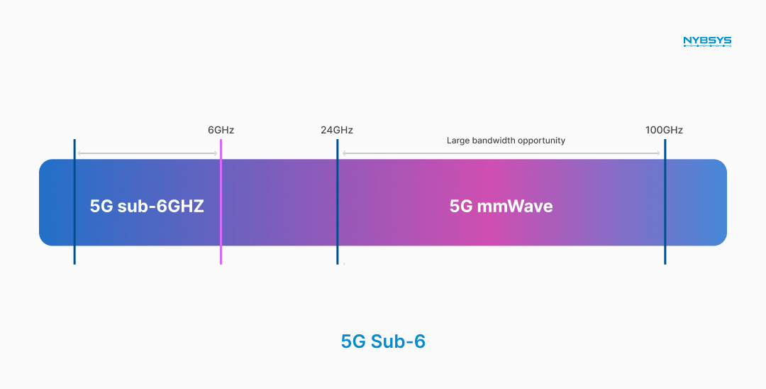
Figure 1. Sub-6 GHz and UWB frequency bands for 4G/5G wireless systems

Figure 2. Evolution of mobile wireless communication technologies
LITERATURE SURVEY
Over the last several years, there has been much research that has been dedicated to the development of compact wideband and UWB antennas to be used in modern wireless communication systems, specifically in the sub-6 GHz 4G/5G frequency band and beyond. Fed planar slot and patch antennas is one of the most popular antenna structures to be studied because they have low profile, are easy to fabricate and can be integrated. Conventional designs are however known to have limited impedance bandwidth and comparatively low gain that have driven the need to explore different methods of optimisation, including DGS, slot cuts, directors, and parasitic elements to improve performance. The literature has already presented a number of studies as some are enumerated below. Liton Chandra Paul et al. (2022) described a plus-shaped patch antenna with a slotted patch in it and a DGS to use in 5G sub-6 GHz and WiMAX. The authors modeled the antenna using a Rogers RT5880 material and showed that the antenna has a wide impedance band between 2.67 and 5.23 GHz with a peak gain of about 4.65 dB which confirms that slot structures combined with DGS can be effectively used in terms of bandwidth enhancement [36]. After this contribution, by the authors Dhawan Singh et al. (2025) introduced a hexagonal-slotted wideband Coplanar Waveguide (CPW)-fed microstrip antenna that is 5G network-optimized. The authors used various slot designs to drive various resonant modes and had a simulated bandwidth of 3.7 to 8.5 GHz, hence validating that slot-based modifications are effective in enhancing impedance bandwidth [37]. Mohamed Lemine El Issawi et al. (2024) examined wideband microstrip patch antennas that have defected ground structures to utilize at sub-6 GHz. The authors pointed out that DGS is an important device in improving the impedance matching and bandwidth performance with special importance to the effectiveness of the ground-plane modification methods in planar antenna designs [38]. Naser O. Parchin et al. (2020) suggested a UWB microstrip-fed slot antenna that has a better bandwidth and dual band-notched with the help of protruding parasitic strips on an FR-4 substrate. The authors showed that added slots and parasitic elements were effectively integrated to provide a broad impedance bandwidth of 2.5 to 15 GHz with the two-banding suppression, which is the usefulness of parasitic structures in the widening of impedance bands [39]. IU Din et al. (2023) developed and modelled a small UWB circular monopole antenna using a gain enhancement frequency selective surface (FSS) in addition to a frequency selective surface (FSS). The authors have noted significant gain enhancement at constant wide band of impedance, which indicates the possibilities of external periodic structures in enhancing radiation properties [40]. TO Olawoye et al. (2022) introduced a high-gain wideband microstrip patch antenna to be used in sub-6 GHz 5G applications. The authors showed that with optimized radiator geometry and ground-plane design wide bandwidth and dramatic gain improvement can be attained, and the structural optimization of next-generation wireless antennas is important [41]. Ajay Singh et al. (2024) designed a microstrip patch antenna fed with a microstrip line and made in the form of a rectangle shaped slot that is DGS-based in 5G communication system. The authors obtained tri-band operation with the highest gains of up to 11.37 dB at desired frequencies, which means that slot structures in combination with DGS are effective in multi-band operation and gain enhancement [42]. MF Ahmed (2025) has done a detailed review of methods of increasing gain and bandwidth in ultra-wideband patch antennas made using microstrip. The author has examined different methods such as frequency selective surfaces, defected ground designs, and parasitic elements, and has concluded that the methods can be applied to offer effective solutions in bandwidth extension and gain enhancement in wideband antenna designs [43]. W. Sun (2021) suggested a gain stabilization and gain improvement methodology of wideband slot-coupled microstrip antennas by using reflector-plus-sidewall structure. The author showed that the optimized design had a broad band of impedance with a flatter and an increased gain response within the operating band [44]. Finally, Junho Yeo and Jong-Ig Lee (2023) have also shown gain improvement in microstrip patch array antennas through the addition of metallic plates on the axis of the array. The authors indicated a significant peak gain increase of up to 7 dB and demonstrated that further structural components can work well to regulate the radiation properties and increase antenna gain [45].
Table 1 provides a comparative overview of the state of the representative research on the design of wideband and gain-enhanced microstrip antenna designs, showing design methodologies used as well as the performance in terms of impedance bandwidth and gain. The articles analysed show that, defected ground structures, slot-based radiators, parasitic elements, frequency selective surfaces, reflector-assisted designs, etc. can be effectively used to improve the performance of an antenna. Nonetheless, numerous designs that have been reported are limited in frequency coverage, complexity, or use of multilayer and expensive substrate. The presented observations explain why compact, low-cost, and wideband antenna solutions are required that can offer stable radiation properties and enhanced gain over a large frequency band, which is why the proposed antenna is developed.
Table 1. Summary of related works on wideband microstrip antenna designs.
Authors & Ref. | Year | Proposed Method | Obtained Results |
Liton Chandra Paul et al. [36] | 2022 | Slotted plus-shaped microstrip patch antenna with defected ground structure (DGS) | Bandwidth of 2.67–5.23 GHz with peak gain ≈ 4.65 dB |
Dhawan Singh et al. [37] | 2025 | Hexagonal-slotted CPW-fed microstrip antenna | Wide impedance bandwidth from 3.7–8.5 GHz |
Mohamed L. El Issawi et al. [38] | 2024 | DGS-based wideband microstrip patch antenna | Improved impedance matching and enhanced bandwidth for sub-6 GHz |
Naser O. Parchin et al. [39] | 2020 | Microstrip-fed slot antenna with parasitic strips | UWB operation from 2.5–15 GHz with dual band-notched characteristics |
IU Din et al. [40] | 2023 | UWB monopole antenna with frequency selective surface (FSS) | Wide bandwidth with noticeable gain enhancement |
T. O. Olawoye et al. [41] | 2022 | Geometry-optimized high-gain microstrip antenna with DGS | Wideband operation with significant gain improvement for sub-6 GHz |
Ajay Singh et al. [42] | 2024 | Rectangular-slot DGS microstrip patch antenna | Tri-band operation with peak gain up to 11.37 dB |
M. F. Ahmed [43] | 2025 | Review of gain and bandwidth enhancement techniques for UWB antennas | Identified effective methods including DGS, FSS, and parasitic elements |
W. Sun [44] | 2021 | Slot-coupled antenna with reflector and sidewall structure | Wide bandwidth with stabilized and enhanced gain response |
J. Yeo and J.-I. Lee [45] | 2023 | Patch array antenna with metallic plate directors | Peak gain enhancement of up to 7 dB |
Proposed Methodology
The wideband microstrip-fed planar slot antenna is proposed and designed in a systematic manner through the three-phase systematic approach to design, optimization, and performance improvement. The design is able to achieve a slow-paced enhancement in the bandwidth of impedance and radiation, and a low-cost and compact design is supported. The general development process is summarized in Figure 3 that depicts the key steps of the implemented methodology.
The design of the major antenna structure is done in Phase 1. This step entails characterizing substrate material, ground plane geometry, radiating slot geometry, and microstrip feed size. The basic resonance behaviour is determined by initial simulations, and a basic design that satisfies the basic operation requirements is obtained.
Phase 2 is concerned with antenna optimization by means of iterative parametric testing. Significant geometrical parameters are desired to be varied systematically to enhance impedance matching and expand the bandwidth. This is done by closely observing the reflection coefficient (S11), current distribution, as well as radiation patterns to make sure that the performance of the structure is improved without adding additional complexity to the structure.
Finally, Phase 3 is the phase of performance improvement, and it is the one where structural change that include the refinements of directors and shape are introduced. The additions enhance gain, directivity, and radiation efficiency. To confirm the gains attained, the electromagnetic field analysis is involved.

Figure 3. Proposed Methodology phases
Phase 1: Primary Antenna Design
The design of the reference antenna in the initial stage is done using the basic transmission line approach and microstrip antenna design concepts. The reference antenna is designed on the FR-4 substrate owing to its low cost and easy availability. Starting values of radiating elements, microstrip line, and ground plane are considered to get proper impedance matching at wide bandwidth.
The initial antenna acts as the template upon which the next phase of optimization will be conducted. The simulation results reveal that the proposed antenna will function between 3.25 GHz and 11.6 GHz according to the reflection coefficient criterion  . It implies that impedance matching has been accomplished within this range of frequencies. Nonetheless, more tuning needs to be done in order to improve the lower frequency of operation, bandwidth stability, and radiation capabilities. As such, this reference model sets the foundation for the geometric optimization and gain optimization processes.
Phase 2: Antenna Optimization Using Trial-and-Error Approach
The second phase is aimed at optimizing the reference antenna to enhance the impedance matching and bandwidth continuity. Full-wave electromagnetic simulations were used to run a systematic trial-and-error parametric refinement process. The key adjusted parameters at this phase were the radiator profile, slot size and slot position, the position of the feed-line, the length and width of the feed-line arm, the size of the partial ground-plane, and the size of the defected ground structure.
The radiating element is gradually modified from the initially designed reference geometry into a tapered and curved profile to increase the effective current path and excite additional resonant modes. The slot layout and feed-line geometry were then tuned to enhance electromagnetic coupling and provide a smoother impedance transition between the 50 Ω input port and the radiating structure. In addition, the partial ground plane and L-shaped defected ground structure were refined to control fringing fields and reduce impedance mismatch.
The designs were tested on each iteration with respect to the simulated reflection coefficient (S11), the distribution of currents on the surfaces, gain response, and the radiation pattern behavior. In this refinement, various resonant modes were created and added together to form better impedance bandwidth and some better foundation to the final gain-enhancement step.
Phase 3: Antenna Enhancement Using Directors and Performance Validation
At the last stage, three rectangular directors of a small size are placed in front of the radiating structure to improve the radiation performance of the optimized antenna. Such parasitic components are added to guide the radiated energy in a more efficient manner and enhance the overall gain of the antenna without raising the size and the complexity of the antennas too much. The improved antenna design is next tested to confirm its functionality in the aspects of impedance band, gain and radiation patterns. The final design has a continuous -10 dB band of impedance of 2.7 to 12 GHz. Gain performance is investigated in three representative frequency bands ensuring an observable increase in gain with values of about 5.53 to 6.97 dB, and still achieving good impedance matching and constant radiation performance. The findings confirm the usefulness of the suggested methodology to reach a small, wideband, and gain-enhanced antenna, which can be used in the context of the current broadband wireless communication systems.
ANTENNA DESIGN AND OPTIMIZATION
This section of the paper describes the proposed antenna design procedure based on the analytical transmission-line equations and the validations through full-wave electromagnetic simulations using Ansys High Frequency Structure Simulator (HFSS).
Reference Patch Design
The antenna design cycle starts with the standard rectangular patch of microstrip, which is used as a reference figure with which the initial radiator size is calculated. Though the end antenna design has moved to a slot-based wideband design, the classical patch model offers a good analytical base and correct impedance behaviour before bandwidth-enhancement variations.
The antenna is implemented on a low-cost FR-4 substrate with a relative permittivity  , loss tangent
  , and thickness
  . For a selected fundamental resonant frequency
  , the patch width
  is calculated using transmission-line theory, which presented by means of the following Equation [46][47]:
| 
| (1) |
where  is referring to the speed of light in free space. The effective constant of the dielectric material
  , which determined for fringing fields at the patch edges, is given by mean of the following Equation [48]:
| 
| (2) |
Due to the fringing-field effect at the radiating edges, the effective resonant length becomes greater than the physical patch length corresponding to the fundamental mode, and it can be expressed by the following Equations [49]:
| 
| (3) |
This extension in the length arises from fringing-field effects; consequently, the physical patch length is appeared slightly shorter than the effective resonant length. In mathematical form, the length extension  is calculated as follows [30]:
| 
| (4) |
Finally, the actual patch length  of the antenna can be mathematically obtained by means of the following Equation [50]:
| 
| (5) |
The reference rectangular patch dimensions are calculated using the classical transmission-line model at the design frequency  GHz. The patch width is determined to optimize radiation efficiency, while the effective dielectric constant accounts for the fringing fields at the patch edges. The effective resonant length is then calculated, and a length correction factor is applied to account for fringing effects, yielding the physical patch length. These analytical expressions provide the initial dimensions of the radiating element, which are summarized in Table 2.
Table 2. Design parameters and calculated dimensions of the proposed antenna
Category | Parameter | Symbol | Value |
Substrate | Relative permittivity | 
| 4.4 |
Substrate thickness |
| 1.6 |
Reference radiator (top) | Patch width |
| 13.04 |
Effective permittivity |
| 3.781 |
Effective resonant length | 
| 11.02 |
Fringing length extension |
| 0.718 |
Physical patch length |
| 9.58 |
Defected ground plane (bottom) | Rectangular section size | 
| 
|
L-shaped DGS short arm length | 
| 4.66 |
L-shaped DGS short arm width | 
| 0.8 |
L-shaped DGS long arm length | 
| 11.6 |
L-shaped DGS long arm width | 
| 1.9 |
Feed Line Design and Excitation Mechanism
The proposed antenna is excited using a microstrip transmission-line feed, selected for its planar configuration, ease of fabrication, and compatibility with printed circuit board technology. The feed line is designed to provide a characteristic impedance of 50 Ω, ensuring proper matching with standard RF sources. The characteristic impedance  of the microstrip feed line is determined using conventional microstrip transmission-line equations, expressed as [31][32]:
| 
| (6) |
| 
| (7) |
where  denotes the width of the microstrip feed line, is the substrate thickness, and is the effective dielectric constant.
In order to attain wideband impedance matching, the feed line is designed in an adapted stepped and bent design. This is an L-shaped microstrip strip, with a rectangular section of coupling that is incorporated into such a rectangle, with the geometrical dimensions as described in Table 3. The L-shaped feed has long and short arms which are of different width and length to create an effective impedance transforming network between the radiating patch and the 50 Ω. The rectangular shape is designed to maximise capacitive coupling at the feed-radiator junction and the bent design maximises the effective electrical length of the feed path but does not require any increase in the size of the antenna itself. It is an electromagnetically coupled, multiple resonant-mode-excited, gradual-impedance-transitioning, modified version of the feed structure. Therefore, the antenna shows a better impedance comparison and stable wideband performance in all the operating frequency band.
Table 3. Dimensions of the stepped and bent microstrip feed line.
Feed Component | Parameter | Symbol | Value (mm) |
Rectangular coupling section (ground) | Length | 
| 4.00 |
Width | 
| 4.00 |
L-shaped feed (short arm) | Length | 
| 4.66 |
Width | 
| 0.80 |
L-shaped feed (long arm) | Length | 
| 11.60 |
Width | 
| 1.90 |
Optimization Through Parametric Refinement and Shape Modification
The proposed antenna is approached based on the initial analytical design in which the wideband performance of the proposed antenna is acquired through a systematic trial and error optimization in Ansys HFSS by repeatedly correcting and refining the original reference configuration. This type of optimization is performed using a controlled change in the geometry of the radiator, the structure of the feed-line and the configuration of the ground plane, with the results of the electromagnetic simulation.
As Figure 4 shows, the development of the antenna starts with an example of a conventional rectangular patch radiator, which has been used as a reference geometry. Even though this is a predictable basic resonance design, this design is necessarily limited in bandwidth. To overcome this drawback, the reference structure is corrected in successive geometries by creating smooth, tapered, and curved edges of the radiator, creating a geometry inspired by Vivaldi. Such changes are gradually initiated by trial and error to lengthen the effective electrical length in order to allow a gradual impedance change.
Simultaneously, the feed-line configuration is refined, as shown in Figure 5, by adjusting the stepped and bent microstrip geometry to improve coupling between the feed and the radiator. The dimensions and orientation of the feed structure are iteratively tuned to correct impedance mismatch observed in the reference design. In addition, the partial defected ground plane is modified by varying its truncation length and L-shaped profile to enhance fringing fields and strengthen electromagnetic interaction with the top radiating element.
The designs are tested using the simulated reflection coefficient and surface current distribution. By making a series of correction steps to the original reference design, resonant modes are created and successfully combined to create a continuous wideband impedance response. Through this optimization process, there is a huge enhancement in impedance bandwidth and radiation stability and the final antenna configuration is the one shown in the above Figure 4 and Figure 5.
After the optimization of the shape the next step that is taken is to further change the antenna geometry by converting the radiator to a butterfly (bow-tie)-like geometry, and adding sawtooth characteristics to the radiate profile edges, as shown in Figure 6. The shape is influenced by the bow-tie shape increasing the effective aperture of the radiator and enhancing higher field development towards the uncovered part of the antenna which is good in the case of broadband radiation. Also, the sawtooth edge structure presents numerous current discontinuities extending the current path on the surface as well as creating more resonant modes in the operating band. These geometric modifications combined are used to increase electromagnetic coupling between the radiator and the defected ground plane, increase impedance matching and stabilize radiation properties. Subsequently, the antenna attains a better bandwidth continuity and overall performance that allows it to operate in wideband over a wide frequency.
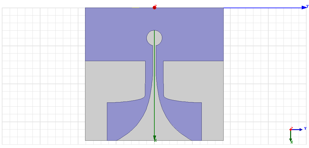
Figure 4. Proposed antenna inside HFSS simulation environment
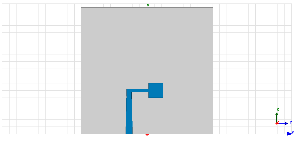
Figure 5. Modified feed line structure for the proposed antenna
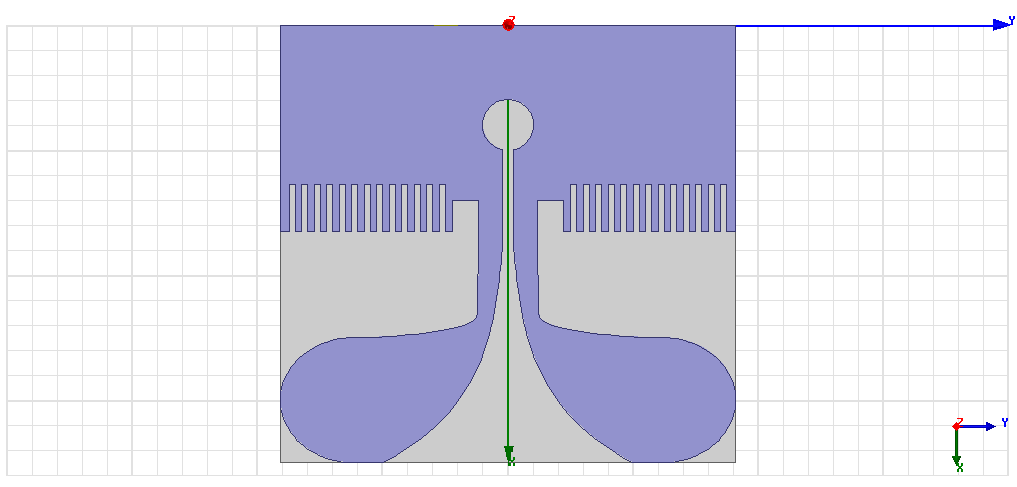
Figure 6. Butterfly-shaped antenna geometry
Gain Enhancement Using Director Elements
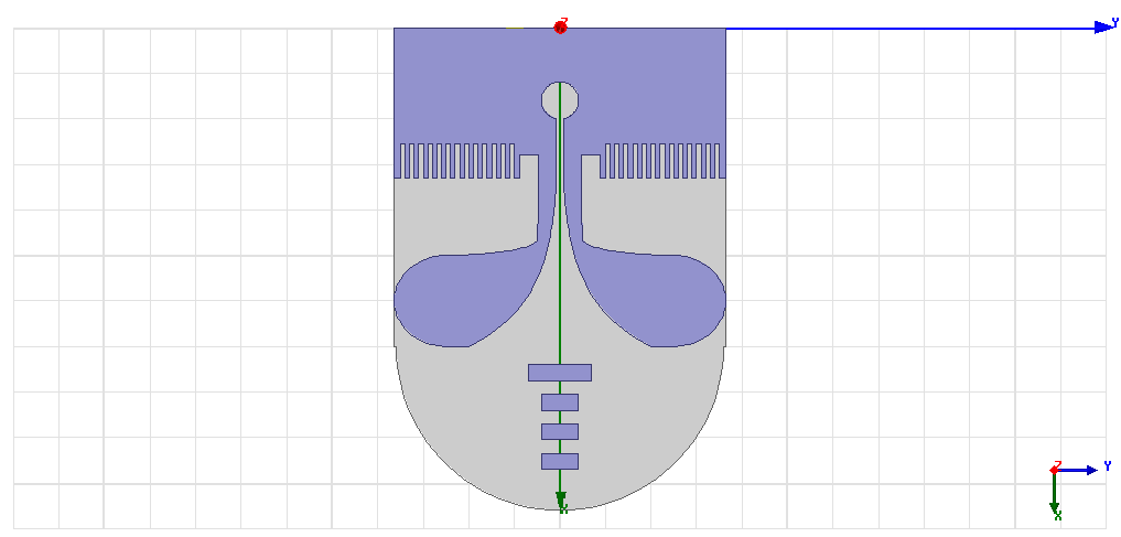
For the additional enhancement in terms of gain and directivity characteristics of the designed antenna, the following three rectangular parasitic directors have been included on the radiating surface of the antenna as illustrated in Figure 7. These directors are aligned successively in front of the main radiator to take the advantage of interaction of electromagnetic fields to channelize the maximum amount of energy in forward direction. The directors are equally spaced from each other by 1.5 mm. This separation was determined using parametric modeling so as to create a constructive interaction between the radiator and the directors, without creating excessive mutual interaction that can affect the impedance characteristics. Furthermore, the separation between the radiator and the first director is kept constant at 23 mm. This separation value ensures optimized performance in terms of high directivity as well as wide impedance bandwidth. These director elements provide a passive guidance structure which helps distribute the surface current and enhance the phase matching of the radiated fields. Consequently, the antenna gains improved forward radiating capability, lower backward radiation level, and better gain characteristics in the tested frequency band. In addition, the implementation of three directors leads to enhanced radiation pattern stability at the chosen representative frequencies of 6.7 GHz, 8.7 GHz, and 10.7 GHz. It is hence evident that the application of these director elements provides a convenient method for enhancing gain while maintaining the compact planar form factor of the proposed antenna.
Besides the parasitic directors, the substrate outline is also optimized more into a lens-like profile, to enhance the gain enhancement mechanism further. The substrate is in the form of a lens, which enables transformation of the wavefront to occur gradually and minimizes the effects of edge diffusion, enabling more electromagnetic waves to travel to the area of the open aperture. This geometrical adjustment enhances the collimation of the field as well as promotes uniformity of phase distribution throughout the radiating aperture, which is advantageous, especially with wideband and high-gain operation.
The synergistic combination of the director elements and the modification of the lens-shaped substrate to achieve a much higher gain and directivity of the radiated antenna, while preserving the broad spectrum of impedance bandwidth and near-constant radiated characteristics. The result of this last optimization phase is a high-performance antenna configuration that can be used in the case of the broadband wireless communication application.
Figure 7. Proposed antenna with parasitic directors and lens-shaped substrate
OBTAINED RESULTS AND DISCUSSION
This section presents and discusses the simulated performance of the proposed antenna by analyzing the S11, gain response, and radiation characteristics of both the initial reference antenna and the final optimized design. The comparison is intended to clarify the influence of the successive geometrical modifications on impedance matching, bandwidth enhancement, and radiation performance. To evaluate the antenna behavior across its wide operating band, three representative frequencies, namely 6.7 GHz, 8.7 GHz, and 10.7 GHz, are selected to represent the lower, middle, and upper regions of the operating range, respectively. At these frequencies, the gain and radiation patterns are investigated to identify the frequency points associated with the reported gain values and to verify whether the antenna maintains reasonably stable radiation behavior across the band. This analysis provides a more rigorous assessment of the effectiveness of the proposed optimization and gain-enhancement techniques.
Return Loss Results for the Reference Antenna
The anticipated results of the simulated S11 confirm that the primary (reference) antenna design has good wideband impedance characteristics. As illustrated in Figure 8, the antenna has an impedance bandwidth of  dB between about 3.25 GHz and 11.6 GHz which translates to an absolute bandwidth of close to 8.35 GHz. This broad operating range allows some of the critical wireless communication bands to be covered such as 4G LTE, sub-6 GHz 5G, and some of the upper microwave spectrum.
It is well seen within this frequency range that there are numerous resonant modes, with deepest impedance minima at 8.7 GHz and 10.7 GHz, where the reflection coefficient is much less than -30 dB. Such resonant reactions are a good sign of effective electromagnetic interaction between the feed line, radiating patch and the defected ground structure. The stimulation and combination of these resonant modes are important in the realization of the broadband of impedance range as noted in the reference design.
Although the wideband behaviour is favourable, slight impedance difference can be observed around the lower and upper band edges, and it can be assumed that the impedance stability and radiation efficiency can be improved further. The following optimization is carried out on the antenna geometry based upon these characteristics and it is in an attempt to increase the gain performance and ensure constant impedance across the entire operating band. In general, the reference antenna defines a strong baseline design of the optimized designs in the subsequent sections.
A major improvement in the performance of the antenna is provided after a long process of parametric optimization and systematic modifications of the shape. There is an optimization process that entails various trial-and-error variations of the radiator geometry, the feed-line layout and the ground-plane characteristics resulting into enhanced impedance matching and bandwidth continuity. Due to these optimizations, the antenna is characterized by a significantly broader -10 dB impedance bandwidth between 2.72 GHz and 12 GHz which is a significant improvement over the primary reference design. This broad span of operations allows it to cover a range of sub-6 GHz 4G and 5G frequencies efficiently and more broadband services at higher frequencies. This has been made possible by the incorporation of parasitic directors, introduction of sawtooth edges into the radiator boundaries, and transformation of the antenna front profile to lens-shaped, which has resulted in a higher level of electromagnetic coupling and a smoother transition between the impedance. The net result of these structural improvements is the excitement of many resonant modes which combine to create an overall wideband response as evident in Figure 9 where it can be seen that the impedance matching is much better in the entire operating frequency range.
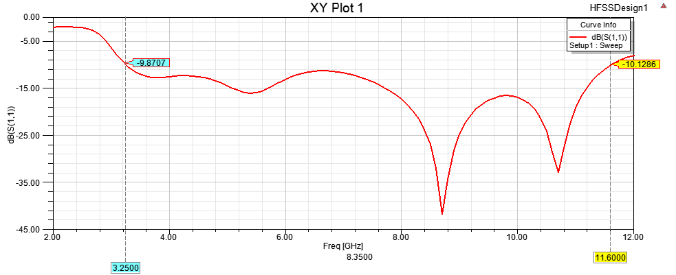
Figure 8. Return loss results for the reference antenna design
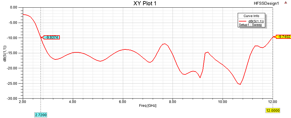
Figure 9. Return loss of the bow-tie-inspired antenna with directors and lens-shaped modification
Gain Result for the Reference Antenna
The proposed antenna has a wide frequency range and therefore a comparative study of the reference antenna and optimized design is conducted at three frequencies points to clearly illustrate the effect of the structural changes. These frequencies are chosen as 6.7 GHz, 8.7 GHz and 10.7 GHz (they are within the effective operation band of the antenna and reflect its broadband behaviour). In the case of the reference antenna, the peak gain of the simulated antenna at 6.7 GHz is about 4.75 dB, which means that the radiation was acceptable in the lower part of the band. The gain at higher frequencies is better, at 8.7 GHz, the gain is 5.28 dB, indicating a higher radiation efficiency in the mid-band frequency band. The highest gain of the reference antenna attains a value of about 5.98 dB at the higher frequency of 10.7 GHz indicating the consistent gain operation within the entire operating range. All three of these radiation features are shown in Figure 10 to Figure 12 which display the simulated gain distributions of the reference antenna at the chosen frequencies. The measured outcomes show that the reference design has a stable and good gain behaviour in a large band and forms a strong base when considering the improvements made in the optimization of the antenna design.
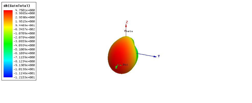
Figure 10. Gain results for the reference antenna at  GHz
GHz
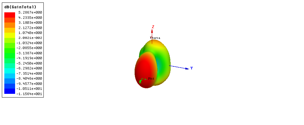
Figure 11. Gain results for the reference antenna at  GHz
GHz
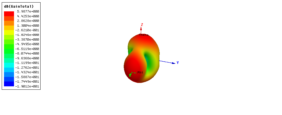
Figure 12. Gain results for the reference antenna at  GHz
GHz
In the optimized and final antenna design, including a bow-tie inspired radiator, a parasitic director and a lens shaped modification to the substrate, a marked increase in the gain performance is obtained at the chosen comparison frequencies. The optimum gain of the optimized antenna at 6.7 GHz is about 5.53 dB, which is a measure of the high radiation efficiency at the lower part of the operating range. The gain further rises to approximately 6.97 dB at 8.7 GHz which demonstrates the high contribution of the director elements and enhanced collimation of the wavefront by the lensed change of shape. The antenna behaviour at higher frequencies ensures that the gain of the antenna remains high with a value of around 6.19 dB with stable radiation behaviour in the upper part of the wide operating band. All these improvements can be easily detected in the gain radiation patterns of the three-dimensional patterns given in Figure 13 to Figure 15 which have a more focused front radiation and a lower back-lobe than those of the reference antenna.
Finally, the results that have been obtained indicate the significant improvement in gain at the chosen frequencies, which proves the design of the final optimized antenna to be much better than the reference design. Although the optimized antenna has a smaller and smoother geometry, it has a better gain performance, suggesting that the shape optimization implemented, integration of the directors and lens-shaped modification can be used to enhance the characteristics of radiations without increasing the size of the antenna. This performance enhancement shows that the proposed design solution is an effective solution to compact, wideband, and gain enhanced antenna applications.
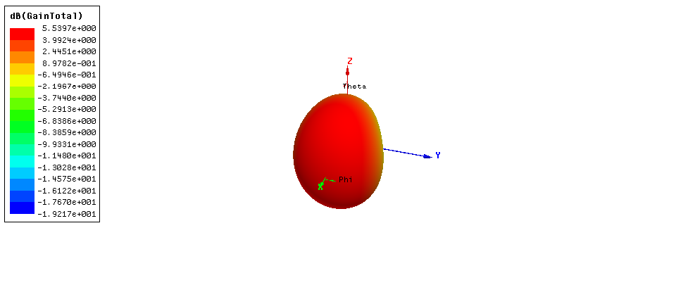
Figure 13. Bow-tie-inspired antenna with directors and lens-shaped modification gain at GHz
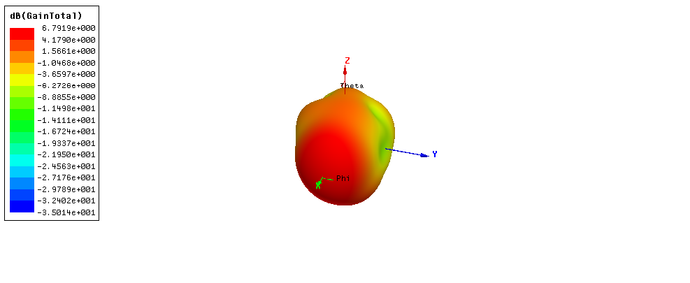
Figure 14. Bow-tie-inspired antenna with directors and lens-shaped modification gain at GHz
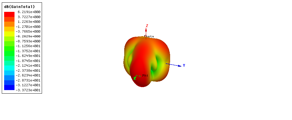
Figure 15. Bow-tie-inspired antenna with directors and lens-shaped modification gain at GHz
PERFORMANCE COMPARISON
The received results indicate significant improvement of the performance of the entire antenna, which proves the usefulness of the given optimization plan. The final antenna has a clear improvement in the impedance bandwidth and the gain characteristics as compared to the reference design. Specifically, the optimized antenna has a much broader -10 dB impedance bandwidth of 2.72 GHz to 12 GHz which is a significant increase over the bandwidth of the reference antenna. The high operating range allows the antenna to utilize many wireless communication bands with a constant impedance that is matched. Besides the enhancement of the bandwidth, the optimized antenna also has higher gain values at the target representative frequencies of 6.7 GHz, 8.7 GHz and 10.7 GHz, and with gain enhancement being consistent at the lower, middle and upper part of the operating band. These enhancements in performance have been explained by the composition of bow-tie-inspired radiator geometry, sawtooth edge modification, parasitic director integration, and lens-shaped substrate profile, which each contribute to better performances in terms of electromagnetic coupling, effective radiating aperture, and better collimation of the wavefronts. The comparison of the impedance bandwidth and gain performance of the reference and optimized antenna designs is summarized in Table 4, which clearly shows that the final antenna design is much better than the reference design in providing wideband and gain-enhanced operation in a small structural footprint.
Table 4. Comparison of S₁₁ bandwidth and gain performance for reference and optimized antennas.
Parameter | Reference Antenna | Optimized Antenna |
−10 dB Impedance Bandwidth | 3.25–11.6 GHz | 2.7–12 GHz |
Gain at 6.7 GHz | 4.75 dB | 5.53 dB |
Gain at 8.7 GHz | 5.28 dB | 6.97 dB |
Gain at 10.7 GHz | 5.98 dB | 6.19 dB |
Size | Acceptable | Compact with better performance |
The gains obtained by the reference antenna and the optimally designed bowtie-inspired antenna are depicted in Figure 16 for three selected frequencies, which are 6.7 GHz, 8.7 GHz, and 10.7 GHz. The selection of these particular frequencies was done in order to investigate the gain performance of both antennas in the lower, middle, and upper frequency bands of operation. As can be observed, higher gain performance is obtained by the optimally designed antenna at each of the considered frequencies.
The gain of the optimized antenna increases to 5.53 dB from 4.75 dB for the reference antenna at 6.7 GHz, reflecting better radiation characteristics of the optimized antenna at the bottom end of the frequency range. The biggest increment in gain is experienced at 8.7 GHz, from 5.28 dB to 6.97 dB. Such an increase in gain is caused by the contribution of several factors, such as the bow-tie-shaped structure of the radiator, the presence of the saw-tooth edge, parasitic directors, and the shape of the substrate. These features contribute to a larger aperture for radiation, as well as to forward radiation in particular. Finally, at 10.7 GHz, the gain remains slightly higher at 6.19 dB compared with 5.98 dB for the reference antenna.
In general, it can be observed that there is always an increase in the gain at the chosen representative frequencies while ensuring broadband performance. These findings clearly prove that the use of the adopted optimization technique has positively affected the performance of the antenna, without reducing its impedance bandwidth.
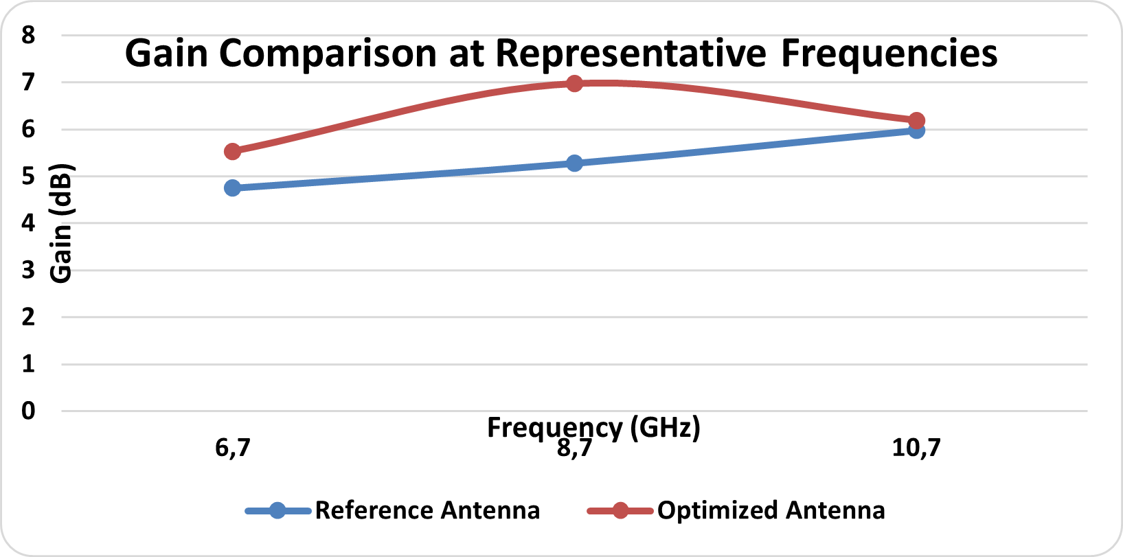
Figure 16. Gain results comparison for the designed antennas
Figure 17 presents a consolidated comparison of the reference and optimized antenna designs by jointly illustrating the impedance bandwidth and gain behaviour at representative operating frequencies. The comparison demonstrates that the optimized antenna achieves an improved performance balance by simultaneously extending the usable bandwidth and enhancing radiation characteristics. A consistent gain improvement is observed across the selected frequencies of 6.7 GHz, 8.7 GHz, and 10.7 GHz, indicating that the applied design modifications are effective over the entire operational range rather than being limited to isolated resonant points. These improvements can be attributed to the redistribution of surface currents and the enhanced directional radiation introduced by the bow-tie–inspired geometry, parasitic directors, and lens-shaped substrate profile. Moreover, the comparison confirms that the optimized antenna maintains stable impedance behaviour while providing higher gain within a compact planar structure, thereby demonstrating its suitability for broadband and multi-band wireless communication applications.
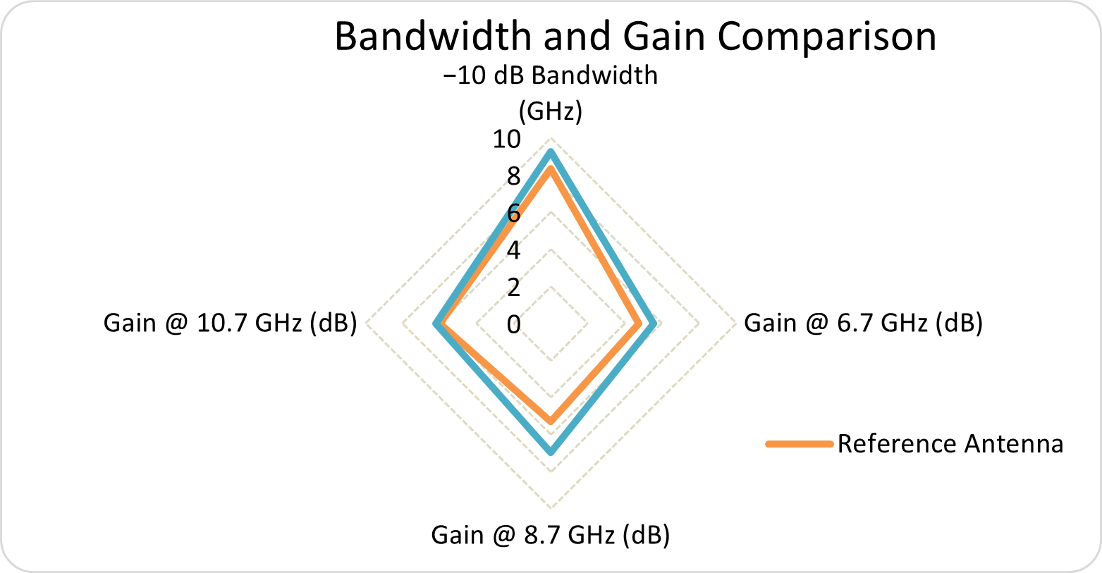
Figure 17. Performance comparison for the designed antennas
CONCLUSION
The paper has focused on the design and optimization with the performance analysis of compact planar antenna operating in wideband with a bow-tie type of radiator structure using parasitic bow-tie directors and a modification of the lens shape on the substrate. The antenna design procedure started with a standard rectangular patch design which became a reference design and was gradually enhanced by systematically changing the shape and systematically changing the parameters to defeat the fundamental bandwidth and gain drawbacks of conventional microstrip antennas. It was realized through geometric adjustments, such as tapered and sawtooth edge shaping, optimization of the defected ground, and optimization of the feed-line, that the antenna was optimized to have wideband matching impedance. The eventual optimized design had the capability to operate in a continuous -10 dB impedance bandwidth of 2.72 GHz to 12 GHz which was much higher than the reference antenna which had a bandwidth of 3.25 GHz to 11.6 GHz. Such operating range also allows covering a variety of sub-6 GHz 4G and 5G frequency bands and 5G higher-frequency broadband wireless spectrums. Besides bandwidth enhancement, a significant gain performance was also obtained through the addition of three parasitic directors and change of substrate profile to a lens-shaped profile. The optimized antenna had other higher values in gain in all the set representative frequencies and in this case the gain stood at about 5.53 dB at 6.7 GHz, 6.97 dB at 8.7 GHz and 6.19 dB at 10.7 GHz, all others having lower gain values as compared to the reference design. The effectiveness of the proposed gain-enhancement techniques is supported by the better radiation properties, such as, as increased forward radiation, and lower levels of back-lobe. The optimized antenna is in general better performing than the reference design yet has a small and planar structure that is easy to fabricate. The overall benefits of a broad bandwidth, increased gain, constant radiation behaviour, and low-cost substrate realization make the presented antenna a serious contender in being integrated into current broadband wireless communication systems, including but not limited to 4G, sub-6 GHz 5G and ultra-wideband applications. Finally, as compared with previously reported designs in the literature, the proposed antenna achieves a broad operating bandwidth of 2.7–12 GHz while maintaining a simple planar structure, a low-cost FR-4 substrate implementation, and improved gain performance, without requiring multilayer structures, external frequency-selective surfaces, or complex fabrication techniques.
REFERENCES
- A. Hassan et al., “Design strategies and performance of IoT antennas: A comprehensive review,” Discover Computing, vol. 28, no. 1, p. 39, 2025, https://doi.org/10.1007/s10791-025-09536-y.
- M. S. Khan, A. Iftikhar, R. M. Shubair, A.-D. Capobianco, B. D. Braaten, and D. E. Anagnostou, “Eight-element compact UWB-MIMO/diversity antenna with WLAN band rejection for 3G/4G/5G communications,” IEEE Open Journal of Antennas and Propagation, vol. 1, pp. 196–206, 2020, https://doi.org/10.1109/OJAP.2020.2991522.
- S. Singh, M. Kumar, and R. Kumar, “Powering the future: A survey of ambient RF-based communication systems for next-gen wireless networks,” IET Wireless Sensor Systems, vol. 14, no. 6, pp. 265–292, 2024, https://doi.org/10.1049/wss2.12094.
- T. S. Rappaport, T. E. Humphreys, and S. Nie, “Spectrum opportunities for the wireless future: From direct-to-device satellite applications to 6G cellular,” npj Wireless Technologies, vol. 1, no. 1, p. 8, 2025, https://doi.org/10.1038/s44459-025-00008-9.
- Y. O. Imam-Fulani et al., “5G frequency standardization, technologies, channel models, and network deployment: Advances, challenges, and future directions,” Sustainability, vol. 15, no. 6, p. 5173, 2023, https://doi.org/10.3390/su15065173.
- D. M. John, S. Vincent, S. Pathan, P. Kumar, and T. Ali, “Flexible antennas for a sub-6 GHz 5G band: A comprehensive review,” Sensors, vol. 22, no. 19, p. 7615, 2022, https://doi.org/10.3390/s22197615.
- M. M. Ismail, B. B. Q. Elias, B. S. Bashar, T. A. Elwi, Z. A. Rhazali, and H. Misran, “Frequency reconfigurable using CLRH for 5G sub-6 GHz wireless application,” Iraqi Journal of Information and Communication Technology, vol. 8, no. 3, pp. 62–72, 2025, https://doi.org/10.31987/ijict.8.3.330.
- N. Qasem, H. M. Marhoon, and N. F. Abdul Malek, “A graphene-based rectangular-notched UWB antenna with reconfigurable notch,” International Journal on Engineering Applications, vol. 13, no. 3, 2025, https://doi.org/10.15866/irea.v13i3.24249.
- D. Bepari et al., “Fluid antennas: Pioneering a new era in next-generation wireless communications,” IEEE Communications Surveys & Tutorials, vol. 28, pp. 5596–5631, 2026, https://doi.org/10.1109/COMST.2026.3678505.
- A. Sivasangari et al., “Design and electromagnetic analysis of photonic crystal based microstrip patch antenna for next generation wireless systems,” Scientific Reports, 2026, https://doi.org/10.1038/s41598-026-48569-1.
- A. Hassan et al., “Designs strategies and performance of IoT antennas: A comprehensive review,” Discover Computing, vol. 28, no. 39, 2025, https://doi.org/10.1007/s10791-025-09536-y.
- M. Marzouk, Y. Rhazi, I. H. Nejdi, F.-E. Zerrad, M. Saih, S. Ahmad, A. Ghaffar, and M. Hussein, “Ultra-wideband compact fractal antenna for WiMAX, WLAN, C and X band applications,” Sensors, vol. 23, no. 9, p. 4254, 2023, https://doi.org/10.3390/s23094254.
- Y. Albaihani, R. Akram, E. A. Hajlaoui, A. M. Almohaimeed, Z. M. Almohaimeed, and A. Albaihani, “5.8 GHz microstrip patch antennas for wireless power transfer: A comprehensive review of design, optimization, applications, and future trends,” Electronics, vol. 15, no. 2, p. 311, 2026, https://doi.org/10.3390/electronics15020311.
- M. Edries et al., “Compact and low mutual coupling 4 × 4 wideband MIMO antenna design for 5G millimeter-wave applications,” Scientific Reports, vol. 16, p. 9804, 2026, https://doi.org/10.1038/s41598-026-39770-3.
- M. V. Yadav, C. Kumar R, S. V. Yadav, T. Ali, and J. Anguera, “A miniaturized antenna for millimeter-wave 5G-II band communication,” Technologies, vol. 12, no. 1, p. 10, 2024, https://doi.org/10.3390/technologies12010010.
- K. PriethamjeVithya, L. M. Varalakshmi, S. S., P. K., and S. L. V., “4 port MIMO antenna for 5G and Wi-Fi integration in smart device applications,” in Proc. 2026 6th International Conference on Expert Clouds and Applications (ICOECA), pp. 17–22, 2026, https://doi.org/10.1109/ICOECA68095.2026.11485592.
- J. P. Siyara, M. N. Jivani, S. P. Lavadiya, and S. K. Patel, “Design and diversity parameter analysis of metamaterial-inspired quad-port MIMO antenna structure for sub-6 GHz 5G wireless communication application,” Journal of Electromagnetic Waves and Applications, vol. 40, no. 6, pp. 876–906, 2026, https://doi.org/10.1080/09205071.2025.2611285.
- H. M. Marhoon, H. Al-Rammahi, N. Basil, N. Qasem, and B. M. Tarik, “Towards intelligent control architectures: A systematic review of Internet of Things applications in control systems,” Iraqi Journal of Information and Communication Technology, vol. 9, no. 1, pp. 1–29, 2026, https://doi.org/10.31987/ijict.9.1.373.
- F. A. Salman and B. M. Sabbar, “DOA estimation exploiting moving platform of unfolded coprime array,” International Journal of Intelligent Engineering and Systems, vol. 15, no. 2, pp. 532–542, 2022, https://doi.org/10.22266/ijies2022.0430.47.
- J. MP, T. P. Surekha, and S. Kumar AJ, “Innovative designs and performance evaluation of super wideband MIMO antennas: A survey,” Nondestructive Testing and Evaluation, vol. 41, no. 2, pp. 635–666, 2026, https://doi.org/10.1080/10589759.2024.2447387.
- L. F. Guerrero-Vásquez, N. A. Chacón-Reino, S. D. Tenezaca-Angamarca, P. A. Chasi-Pesantez, and J. O. Ordoñez-Ordoñez, “Advancements in antenna and rectifier systems for RF energy harvesting: A systematic review and meta-analysis,” Applied Sciences, vol. 15, no. 14, p. 7773, 2025, https://doi.org/10.3390/app15147773.
- M. S. Yahya, S. Soeung, S. K. A. Rahim, U. Musa, S. S. B. Hashwan, Z. Yunusa, and S. A. Hamzah, “LoRa microstrip patch antenna: A comprehensive review,” Alexandria Engineering Journal, vol. 103, pp. 197–221, 2024, https://doi.org/10.1016/j.aej.2024.06.017.
- Y. S. Gurbet and S. Doğu, “Comprehensive review of Ku, K, and Ka band antenna designs: Applications in CubeSats,” International Journal of Aeronautical and Space Sciences, vol. 27, pp. 447–496, 2026, https://doi.org/10.1007/s42405-025-00989-5.
- B. Mishra, A. K. Singh, T. Y. Satheesha, R. K. Verma, and V. Singh, “From past to present: A comprehensive review of antenna technology in modern wireless communication,” Journal of Engineering Science & Technology Review, vol. 17, no. 3, 2024, https://doi.org/10.25103/jestr.173.20.
- C. Singh et al., “A comprehensive survey on millimeter wave antennas at 30/60/120 GHz: Design, challenges and applications,” Wireless Personal Communications, vol. 133, pp. 1547–1584, 2023, https://doi.org/10.1007/s11277-023-10828-z.
- A. Alsudani and H. M. Marhoon, “Design and enhancement of microstrip patch antenna utilizing mushroom-like EBG for 5G communications,” Journal of Communications, vol. 18, no. 3, pp. 156–163, 2023, https://doi.org/10.12720/jcm.18.3.156-163.
- B. S. Taha and H. M. Marhoon, “Simulation and manufacturing of modified circular monopole microstrip antenna for UWB applications,” International Journal of Advanced and Applied Sciences, vol. 10, no. 1, pp. 70–78, 2021, https://doi.org/10.11591/ijaas.v10.i1.
- T. Doloi, G. S. Das, P. P. Kalita, Y. Beria, R. Devi, and A. Buragohain, “Compact MIMO antenna employing inductive–capacitive coupling and honeycomb defected ground structure,” AEU – International Journal of Electronics and Communications, p. 156208, 2026, https://doi.org/10.1016/j.aeue.2026.156208.
- H. Ahmadi et al., “Ultra-wideband unidirectional pseudospin-polarized waveguide with dual boundary conditions,” Scientific Reports, vol. 15, p. 6717, 2025, https://doi.org/10.1038/s41598-025-91489-9.
- A. Azzouz, R. Bouhmidi, M. E. Munir, M. Sheraz, T. C. Chuah, and I. E. Lee, “Dual-band terahertz MIMO antenna using DGS for UWB applications,” Results in Optics, p. 100968, 2026, https://doi.org/10.1016/j.rio.2026.100968.
- H. M. Marhoon, N. Qasem, N. Basil, and A. R. Ibrahim, “Design and simulation of a compact metal–graphene frequency reconfigurable microstrip patch antenna with FSS superstrate for 5G applications,” International Journal on Engineering Applications, vol. 10, no. 3, pp. 193–201, 2022, https://doi.org/10.15866/irea.v10i3.21752.
- A. S. Kamel and A. S. Jalal, “Reconfigurable monopole antenna design based on fractal structure for 5G applications,” Iraqi Journal of Information and Communication Technology, vol. 1, no. 1, pp. 177–186, 2021, https://doi.org/10.31987/ijict.1.1.159.
- A. Alsudani and H. M. Marhoon, “Performance enhancement of microstrip patch antenna based on frequency selective surface substrate for 5G communication applications,” Journal of Communications, vol. 17, no. 10, pp. 851–856, Oct. 2022, https://doi.org/10.12720/jcm.17.10.851-856.
- L. C. Paul, S. C. Das, T. Rani, S. M. Muyeen, S. A. Shezan, and M. F. Ishraque, “A slotted plus-shaped antenna with a DGS for 5G Sub-6 GHz/WiMAX applications,” Heliyon, vol. 8, no. 12, p. e12040, 2022, https://doi.org/10.1016/j.heliyon.2022.e12040.
- D. S. First, N. Kashyap, and A. Thakur, “Design and optimization of a hexagonal-slotted wideband microstrip antenna for 5G networks RF energy harvesting,” Franklin Open, p. 100409, 2025, https://doi.org/10.1016/j.fraope.2025.100409.
- M. L. El Issawi, D. Konditi, and A. D. Usman, “Design of enhanced wide band microstrip patch antenna based on defected ground structures (DGS) for sub-6 GHz applications,” Int. J. Electrical and Electronics Research, vol. 12, no. 1, pp. 315–321, 2024, https://doi.org/10.37391/IJEER.120143.
- N. O. Parchin, H. J. Basherlou, and R. A. Abd-Alhameed, “UWB microstrip-fed slot antenna with improved bandwidth and dual notched bands using protruded parasitic strips,” Progress in Electromagnetics Research C, vol. 101, pp. 261–273, 2020, https://doi.org/10.2528/PIERC20040701.
- I. U. Din, W. Ullah, N. A. Abbasi, S. Ullah, W. Shihzad, B. Khan, and D. N. K. Jayakody, “A novel compact ultra-wideband frequency-selective surface-based antenna for gain enhancement applications,” J. Electromagnetic Engineering and Science, vol. 23, no. 2, pp. 188–201, 2023, https://doi.org/10.26866/jees.2023.2.r.159.
- T. O. Olawoye and P. Kumar, “A high gain antenna with DGS for sub-6 GHz 5G communications,” Advanced Electromagnetics, vol. 11, no. 1, pp. 41–50, 2022, https://doi.org/10.7716/aem.v11i1.1670.
- A. Singh and S. Joshi, “Design of Y-shaped tri-band rectangular slot DGS patch antenna at sub-6 GHz frequency range for 5G communication,” Journal of Engineering and Applied Science, vol. 71, p. 144, 2024, https://doi.org/10.1186/s44147-024-00476-w.
- M. F. Ahmed and M. H. Kabir, “An analysis of methods for enhancing gain and bandwidth in ultra-wideband microstrip patch antennas,” Cureus Journals, vol. 2, no. 1, 2025, https://doi.org/10.7759/s44388-025-03326-4.
- W. Sun and Y. Li, “Gain stabilization method for wideband slot-coupled microstrip antenna,” IEEE Transactions on Antennas and Propagation, vol. 69, no. 12, pp. 8932–8936, 2021, https://doi.org/10.1109/TAP.2021.3097441.
- J. Yeo and J.-I. Lee, “Gain enhancement of microstrip patch array antennas using two metallic plates for 24 GHz radar applications,” Electronics, vol. 12, no. 7, Art. 1512, 2023, https://doi.org/10.3390/electronics12071512.
- H. M. Marhoon, H. A. Abdulnabi, and Y. Y. Al-Aboosi, “Designing and analysing of a modified rectangular microstrip patch antenna for microwave applications,” Journal of Communications, vol. 17, no. 8, pp. 668–674, 2022, https://doi.org/10.12720/jcm.17.8.668-674.
- N. Qasem and H. M. Marhoon, “Simulation and optimization of a tuneable rectangular microstrip patch antenna based on hybrid metal–graphene and FSS superstrate for fifth-generation applications,” TELKOMNIKA (Telecommunication Computing Electronics and Control), vol. 18, no. 4, pp. 1719–1730, 2020, https://doi.org/10.12928/telkomnika.v18i4.14988.
- T. Nahar and S. Rawat, “Efficiency enhancement techniques of microwave and millimeter‐wave antennas for 5G communication: A survey,” Transactions on Emerging Telecommunications Technologies, vol. 33, no. 9, p. e4530, 2022, https://doi.org/10.1002/ett.4530.
- A. Tiwari, A. A. Khurshid, and K. Sharma, “Compact wearable microstrip antenna design using hybrid quasi-Newton and Taguchi optimization,” Scientific Reports, vol. 15, p. 116, 2025, https://doi.org/10.1038/s41598-024-83864-9.
- E. D. Hussein, N. Qasem, M. S. Jameel, M. Ilyas and O. Bayat, "Performance Optimization of Microstrip Patch Antenna Using Frequency Selective Surfaces for 60 GHz," 2020 28th Signal Processing and Communications Applications Conference (SIU), pp. 1-4, 2020, https://doi.org/10.1109/SIU49456.2020.9302486.
- H. Wei, W. Chen, J. Lv, G. Shen, and X. Xu, “Compact N-shaped metasurface microstrip antenna designed for the 5G/B5G communications,” International Journal of Communication Systems, vol. 39, no. 1, p. e70309, 2026, https://doi.org/10.1002/dac.70309.
- H. M. Marhoon and N. Qasem, “Simulation and optimization of tuneable microstrip patch antenna for fifth-generation applications based on graphene,” International Journal of Electrical and Computer Engineering, vol. 10, no. 5, pp. 5546–5558, 2020, https://doi.org/10.11591/ijece.v10i5.
Ramy Abduimawjood Mohammed (A Compact Wideband Microstrip-Fed Planar Slot Antenna with Partial Defected Ground Structure for 2.7–12 GHz Wireless Applications)