Buletin Ilmiah Sarjana Teknik Elektro ISSN: 2685-9572
Vol. 8, No. 2, April 2026, pp. 380-394
A Self-Balancing 13-Level Single-Phase Triple Gain Inverter
Sakthisudhursun Balakrishnan, Muralidharan Srinivasan, Sundaramahalingam Subramaniam,
Vanaja Narayanaswamy
Department of Electrical and Electronics Engineering, Mepco Schlenk Engineering College, Sivaksi, Tamilnadu, India
ARTICLE INFORMATION |
| ABSTRACT |
Article History: Received 07 October 2025 Revised 03 February 2026 Accepted 01 April 2026 |
| 
A potential single stage power electronics interface for integrating renewable sources like PV, fuel cells, etc. with an AC load is a switched capacitor based multilevel inverter with boosting capability. In this research, a thirteen-level MLI topology with voltage boosting factor of three a gain of three for the renewable energy integration is proposed. The proposed MLI requires twelve unidirectional switches, one bidirectional switch, three capacitors, and a single DC source. The voltage stress across each switch is lower than the peak output voltage since the proposed inverter doesn't need a back-end H-Bridge. The proper selection of switching sequence enables the self regulation of voltage across all three capacitors, is self-regulated eliminating the need of additional sensor/control. Simulation results obtained from MATLAB/Simulink confirm the stable operation of the MLI and the self-regulation of switched capacitor voltages under step variations in load, source voltage, and modulation index. A comprehensive comparison with existing topologies demonstrates the superiority of the proposed topology in terms of reduced total number of components and lower total blocking voltage. |
Keywords: Boost Inverter; Switched-Capacitor; Self-Balancing; Thirteen-Level Inverter |
Corresponding Author: Sakthisudhursun Balakrishnan Department of Electrical and Electronics Engineering, Mepco Schlenk Engineering College,Sivaksi, Tamilnadu, India, 626005. Email: bss@mepcoeng.ac.in |
This work is licensed under a Creative Commons Attribution-Share Alike 4.0 
|
Document Citation: S. Balakrishnan, M. Srinivasan, S. Subramaniam, and V. Narayanaswamy, “A Self-Balancing 13-Level Single-Phase Triple Gain Inverter,” Buletin Ilmiah Sarjana Teknik Elektro, vol. 8, no. 2, pp. 380-394, 2026, DOI: 10.12928/biste.v8i2.14920. |
- INTRODUCTION
The use of renewable energy sources, such as solar photovoltaic systems, wind energy conversion systems, and fuel cells, requires effective DC to AC conversion. Multilevel inverters, owing to their intrinsic benefits such as decreased dv/dt, decreased voltage stress across the switch, enhanced voltage and current THD, fault-tolerant operation, and decreased common mode voltage, have been suggested for the above-mentioned applications [1]-[6]. Diode clamped multilevel inverters, flying capacitor multilevel inverters, and cascaded H-bridge multilevel inverters are some of the common multilevel inverter topologies [7]-[8]. The primary drawback of standard multilevel inverter topologies is that as the number of levels increases, more number of components become necessary [9].
RDC multilevel inverters employing a single source, reduced source, and switched capacitors without boosting capacity have been described [10]-[16]. Research articles [11]-[15] have discussed in-depth comparisons of various multilevel inverters with fewer devices. However, a common drawback of traditional MLI and RDC MLI is that they can only produce an output voltage that is less than or equal to the input voltage. To overcome this drawback various switched capacitor based boost inverters have been introduced [17]-[32]. The various existing 13-level single-phase MLI with triple voltage gain were discussed in [33]-[36]. Anotherer thirteen level inverter with gain of 1.5 and gain of 6 is briefed in [37]-[39]. A generalized switched capacitor module was proposed in [33] which was combined with a packed H-bridge structure to produce a 13-level output using two sources. The major drawback of this topology is that it requires two supply sources, a higher total blocking voltage and four capacitors to realize a 13-level output across the load. A generalized step-up MLI using crisscross capacitor units was suggested in [34]. Two crisscross units are required for a voltage gain of 3. The main issues are that it requires 4 capacitors and a mix of semiconductor switches with a freewheeling diode and without a freewheeling diode to realize a thirteen level output. A new 13-level MLI was proposed in [35] with less total blocking voltage. But the topology requires 4 additional diodes and 4 switched capacitors to realize 13-level output. The increased number of other components in [35] results in less reliability. A 12-switch based 13-level SC-MLI with the gain of three is proposed in [36]. In addition to power semiconductor switches it requires 3 capacitors and 3 diodes. Decreased efficiency at high power and use of additional diodes are the main problem with the topology [36]. A single source thirteen level K-type MLI is proposed in [37], which requires 4 capacitors to realize thirteen level output with gain of 1.5. It requires mix of semiconductor switch with freewheeling diode and without freewheeling diode. In general, from the above literature study there is need of single source MLI with reduced number of switches and other components such as capacitors and diodes so as increase the reliability efficiency and power density of inverter. This paper therefore introduces a switched capacitor-based MLI topology that achieves gain of three with reduced number of capacitors and incorporates LDN topology to achieve more number voltage levels using fewer switches. The key features of this proposed topology include:
- Utilization of a single DC voltage source
- Only 14 switches are needed to produce a 13-level output (Bidirectional switches are counted as two unidirectional switches while arriving total number of switches)
- A gain of 3
- The maximum voltage stress is limited to 2VDC
- An inherent polarity converter that eliminates the need for a backend H-bridge
- Capacitors are self-balancing, negating the requirement for external sensors.
The rest of the paper is organized as follows: The Section-2 describes the circuit diagram of the proposed topology and its operation. In Section-3 the modulation technique adopted to generate gate pulse is described. The Section-4 describes the Level Doubling Network's self-balancing characteristic along with mathematical expressions. In Section 5, simulation findings under steady and dynamic conditions are provided. In Section 6, we highlight the superiority of this topology over the existing topology and Section-7 summarizes the conclusions of the proposed work.
- CIRCUIT DESCRIPTION
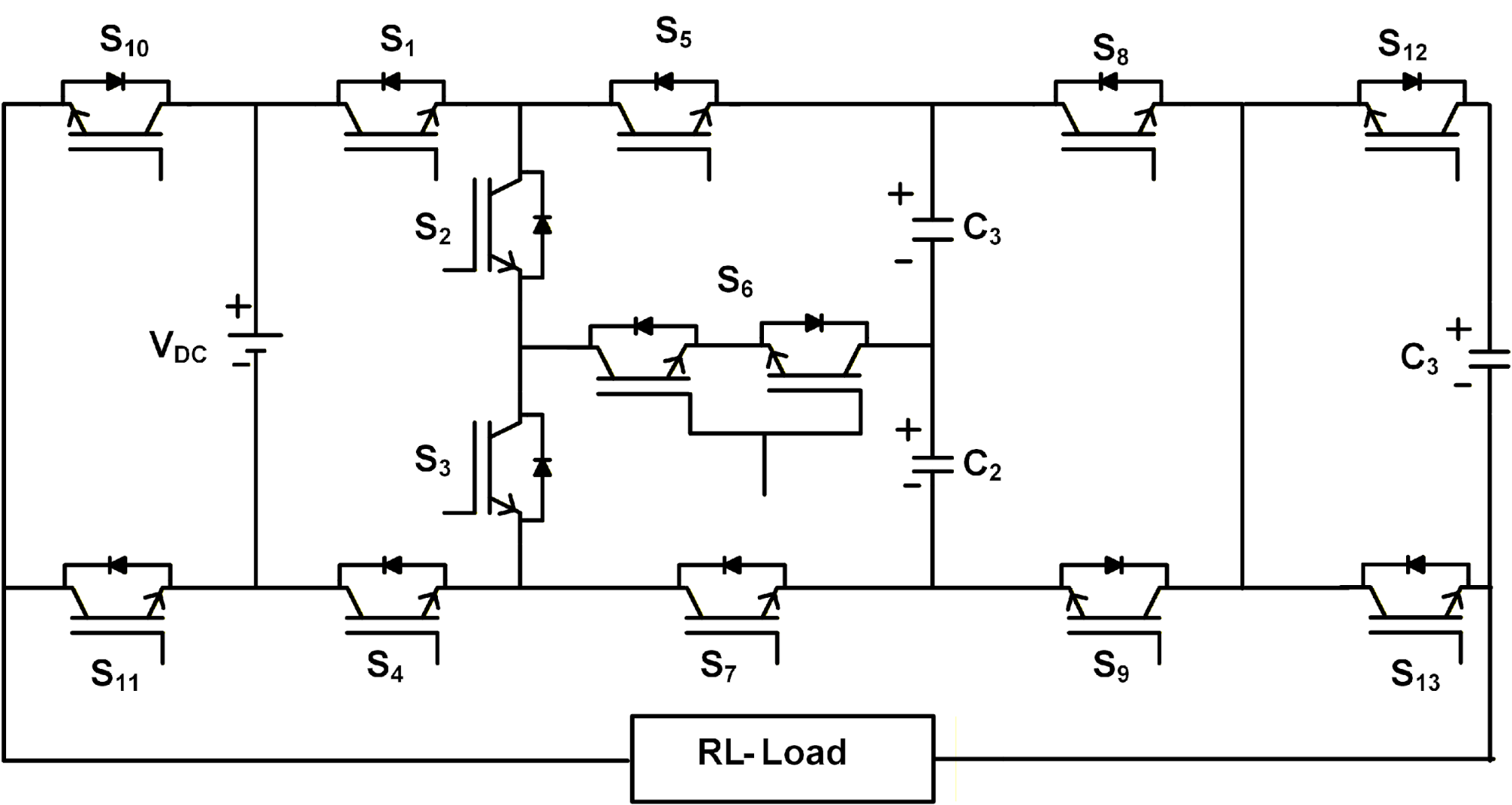
The schematic representation of the proposed boost multilevel inverter topology is depicted in Figure 1. The innovative features of this topology include the requirement of only a single DC source ( ), a boosting factor of three, an integrated polarity generator, and a maximum voltage stress across the switch that is lower than the maximum output voltage. The input DC source can be derived from a fuel cell, battery, or solar PV system. Utilizing the proposed inverter, the following 13 levels can be generated: (
 ). The proposed inverter consists of 12 unidirectional switches, 1 bidirectional switch, and 3 capacitors. Among the 12 unidirectional there are three pairs of complimentary switches (
 ).
).
Figure 1. Structure of proposed topology
The complementary switches must not be activated at the same time to prevent a short circuit of the capacitor or source. The switches  and
and  operate at the fundamental switching frequency. The switch
  is a bidirectional switch realized using a common-emitter configuration, as it offers reduced gate-drive requirements and comparatively lower on-state losses. There are three capacitors: two boost capacitors (
 and
and  ) and one level-doubling capacitor (
 ). The boosting capacitor is connected in parallel to the DC source during the charging phase and in series during the discharging phase. Consequently, the voltage of the boosting capacitors is regulated to match the supply voltage, . The voltage of the level-doubling capacitor is adjusted to be half of the supply voltage by charging and discharging it for equal intervals within one fundamental cycle. As the voltage across the three capacitors is self-regulated, external sensors are not required to achieve this regulation. The various switching states of the proposed inverter are detailed in Table 1. Switches
  , to
, to  ,
,  to
to  and is subject to voltage stresses of , switches
  and
and  to experience a blocking voltage of
  , and switches
  and
and  are subject to a voltage stresses of
  under blocking condition.
Table 1. Switching States of various levels
Switches/Voltage Level |
| 
| 
|
|
|
|
|
|
|
|
|
|
|
+3 | 1 | 1 | 1 | 0 | 0 | 0 | 1 | 1 | 0 | 0 | ↓ | ↓ | - |
+2.5 | 1 | 1 | 1 | 0 | 0 | 0 | 1 | 1 | 0 | 1 | ↓ | ↓ | ↓ |
+2 | 1 | 1 | 0 | 1 | 0 | 1 | 1 | 1 | 0 | 0 | ↓ | ↑ | - |
+1.5 | 1 | 1 | 0 | 1 | 0 | 1 | 1 | 1 | 0 | 1 | ↓ | ↑ | ↓ |
+1 | 1 | 0 | 1 | 1 | 1 | 1 | 0 | 1 | 0 | 0 | ↑ | - | - |
+0.5 | 1 | 0 | 1 | 1 | 1 | 1 | 0 | 1 | 0 | 1 | ↑ | - | ↓ |
+0 | 1 | 0 | 1 | 1 | 1 | 1 | 0 | 1 | 1 | 0 | ↑ | - | - |
-0 | 1 | 1 | 0 | 1 | 0 | 1 | 1 | 0 | 0 | 0 | - | ↑ | - |
-0.5 | 1 | 1 | 0 | 1 | 0 | 1 | 1 | 0 | 0 | 1 | - | ↑ | ↑ |
-1 | 1 | 1 | 0 | 1 | 0 | 1 | 1 | 0 | 1 | 0 | - | ↑ | - |
-1.5 | 1 | 1 | 0 | 1 | 0 | 1 | 1 | 0 | 1 | 1 | ↑ | ↓ | ↑ |
-2 | 1 | 0 | 1 | 1 | 1 | 1 | 0 | 0 | 1 | 0 | ↑ | ↓ | - |
-2.5 | 1 | 0 | 1 | 1 | 1 | 1 | 0 | 0 | 1 | 1 | ↓ | ↓ | ↑ |
-3 | 0 | 1 | 1 | 1 | 1 | 0 | 0 | 0 | 1 | 0 | ↓ | ↓ | - |
Information: “↑” =Charging, “↓” =Discharging, “-” = not affected |
- SINGLE CARRIER BASED MODULATION METHOD
Various methods have been proposed in literature to generate gate pulse for the multilevel inverter [40]–[42]. The performance of the proposed topology is analyzed with the help of single carrier based sinusoidal pulse width modulation proposed in [43] owing to its simplicity, easy implementation and reduced number of comparators compared to conventional level-shifted and phase-shifted PWM schemes. To generate gate pulse for thirteen level inverters using this modulation technique requires single carrier signal ( ) and six reference signals (
 ). The schematic of the modulator is illustrated in Figure 2. The modulation index (Ma) for thirteen- level inverter is defined to be as per [43].
| 
| (1) |
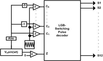
Figure 2. Logic Gate Based Switching Pulse Decoder
In the equation (1),  is the Peak amplitude of modulating signal and
  is the Peak amplitude of carrier signal. All the reference signals are rectified sinusoidal waveforms which are in phase with each other with same frequency and amplitude depending on the required modulation index, but each are offset by a value that is equivalent to the amplitude of the carrier signal. Each of the reference signals is compared with the carrier waveform and six outputs ( to
  ) are obtained. Also, a signum function (
 ) is generated to indicate the positive and negative cycle of the reference waveform. The signum function output is 1 when the reference sinusoidal signal is greater than equal to zero else its output is zero. By applying suitable logic operation of the comparator outputs and signum function particular level information is obtained. The gating pulses for each switch are determined based on the switching states in which they are to be activated, as outlined in Table 1. For example, the switch S8 is turned for entire positive half cycle, hence the logic equation for gating signal is given by,
| 
| (2) |
In same manner the Boolean expressions for the remaining independent switches are given by.
| 
| (3) |
| 
| (4) |
| 
| (5) |
| 
| (6) |
| 
| (7) |
| 
| (8) |
| 
| (9) |
| 
| (10) |
| 
| (11) |
Switches and , and , and and are complementary to each other hence a NOT gate is used in the output of  to generate gate pulse for
  and respectively.
- SELF BALANCING OF CAPACITOR
The self-balancing of the LDN capacitor is accomplished by ensuring it charges and discharges for the same duration within a single fundamental cycle. In this proposed topology, the LDN capacitor discharges during the positive half cycle and charges during the negative half cycle. As the capacitor is charged and discharged for equal interval, the net charge associated with it zero. The charging and discharging current associated with LDN capacitor with load impedance of  are given as per the following equations,
| 
| (12) |
| 
| (13) |
| 
| (14) |
| 
| (15) |
| 
| (16) |
| 
| (17) |
| 
| (18) |
| 
| (19) |
From the expression (19), it is proved that the voltage across the LDN capacitor is regulated to .
- DESIGN OF CAPACITANCE
The values of boost capacitors ( ) are designed based on the longest discharging interval (LDI). For boost capacitor (), the LDI occurs during the positive half of the output voltage and for capacitor () the LDI occurs during the negative half of the output voltage as evident from the Figure 3. As the LDI of both the boost capacitors are same both have same capacitance value. Hence the capacitance computation for () alone is briefed in detail. The capacitance value for () is arrived based on the charge associated with it during the LDI. The charge associated with the capacitor is, where a to b is the LDI of the capacitor (), Im is the peak load current.
where  is calculated by,
| 
| (24) |
| 
| (25) |
The capacitance value is designed by assuming the power factor of 0.85. By substituting the load of 50Ω, 120mH for a ripple 10% of the minimum capacitance required is 2200µF.
- DESIGN OF LDN CAPACITANCE
The charging and discharging of the LDN capacitor are illustrated clearly in Figure 3. As per this, the capacitor charges in negative half cycle and discharges at positive cycle at specific intervals also remains idle in some intervals. The capacitance value of LDN capacitor is arrived based on the procedure and equations as mentioned in [44]. The minimum value of capacitance required is found to be 2200µF.
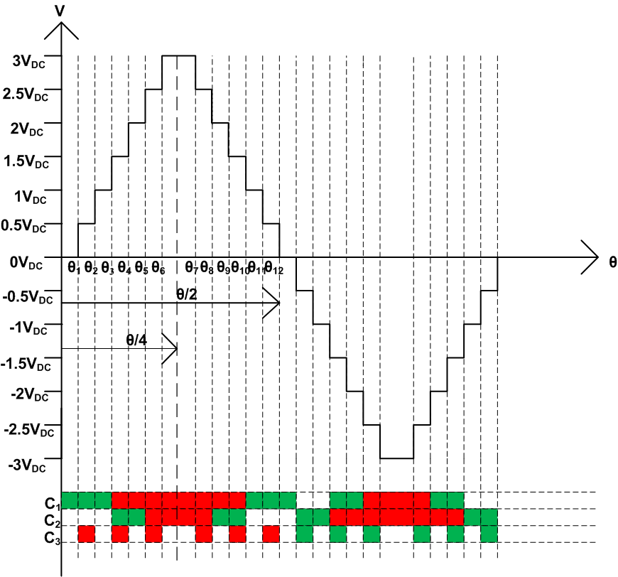
Figure 3. Charging and Discharging states of Switched capacitors
- SIMULATIONS AND RESULTS
To assess the proposed topology's performance, a simulation model is developed using MATLAB SIMULINK. The simulation parameters used in this research are specified in Table 2. Gate pulses for each switch are generated through single carrier-based SPWM, as described in section 3. Figure 4 shows the inverter's output voltage and current waveform in a steady state. The peak output voltage across the load reaches approximately 360V for an input of 120V, confirming the proposed inverter's boosting capability. Figure 5 and Figure 6 depict the steady state voltage across the boost capacitor and LDN capacitor, respectively. The voltage across the boost capacitors is controlled at 120V, while the LDN capacitor is kept at 60V, with voltage ripple of around10%.
Table 2. parameters used in Simulation
Parameters | Values/Ratings |
| 120V |
, , | 2200µF |
Load | 50Ω-120mH |
Output Frequency | 50Hz |
Carrier Frequency | 5kHz |
Modulation Index | 0.95 |
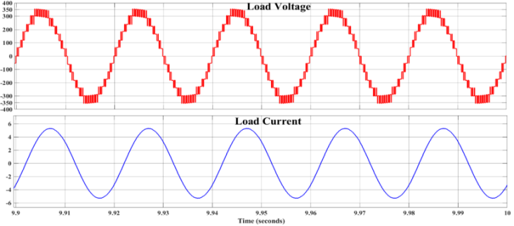
Figure 4. Load voltage and load current for load R=50Ω and L=120mH
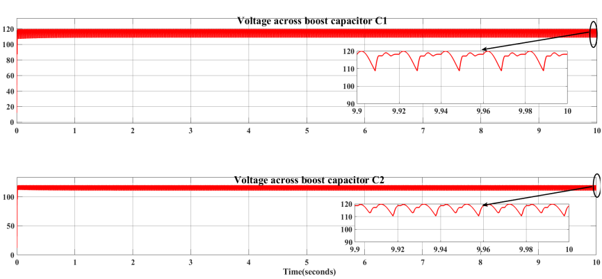
Figure 5. Voltage across Boost capacitors at steady state
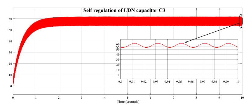
Figure 6. Voltage across LDN capacitor at steady state
To test the effectiveness of self-balancing of capacitors under dynamic condition such as step change in input voltage, load and modulation index are considered in the present study. Figure 7 shows the load voltage and load current during the step change in input voltage. Initially the load voltage is kept as 100V and at time  seconds the input voltage is changes to 120V, the voltage across the boost capacitor is regulated to supply voltage and voltage across the LDN capacitor is regulated to half the supply voltage with allowable ripple as illustrated in Figure 8 and Figure 9 respectively. Figure 10 to Figure 12 shows the load voltage, current and self-regulation of capacitors for the dynamic change in load conditions from
  to
to  load with and
  . During step change from R-load to RL-load, the voltage ripple of capacitors is reduced. According to equation (24) R-load is worst case as far as the ripple across the capacitors, which is validated in the simulation study through the Figure 11 and Figure 12.
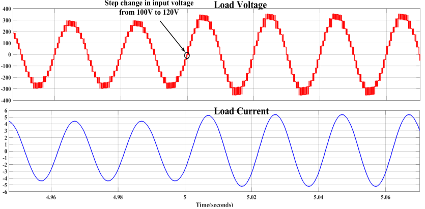
Figure 7. Load voltage and current during step change in source voltage
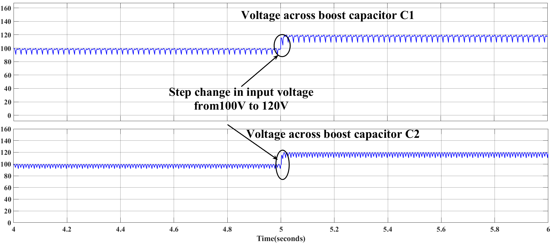
Figure 8. Voltage across Boost capacitors during step change in source voltage
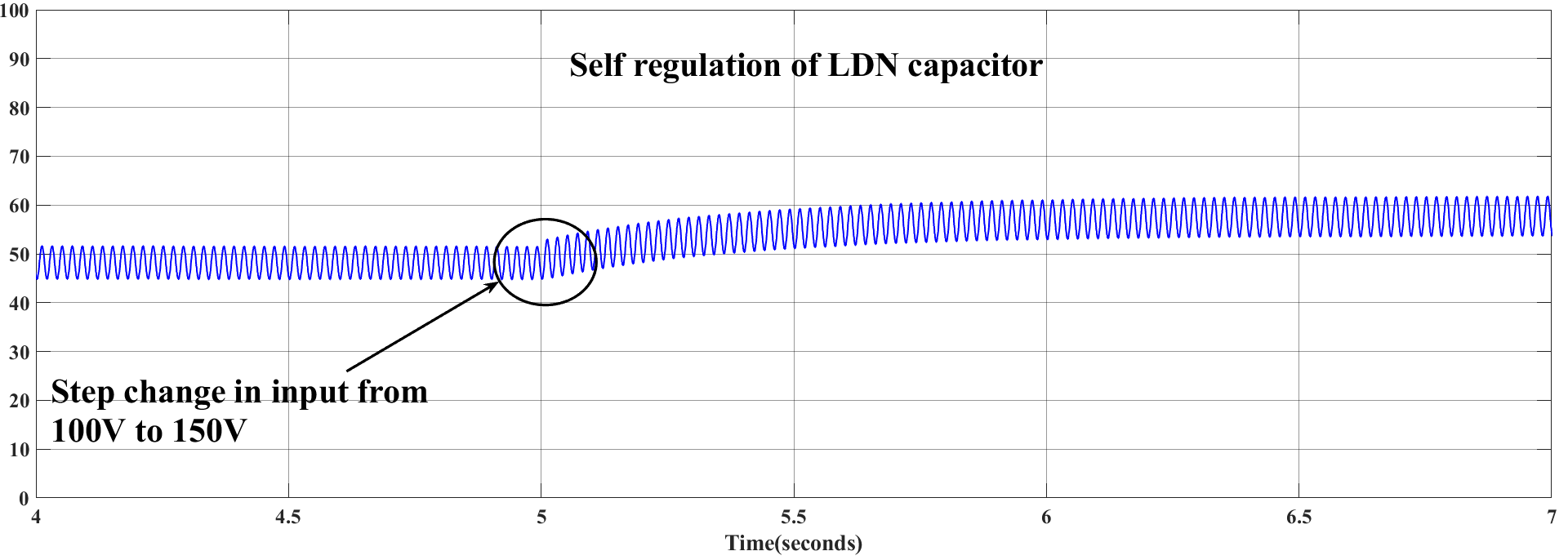
Figure 9. Voltage across LDN capacitors during step change in source voltage
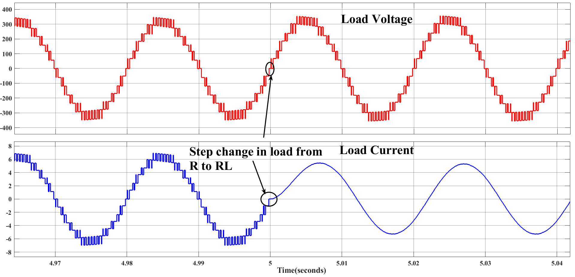
Figure 10. Load voltage and current during dynamic change in load
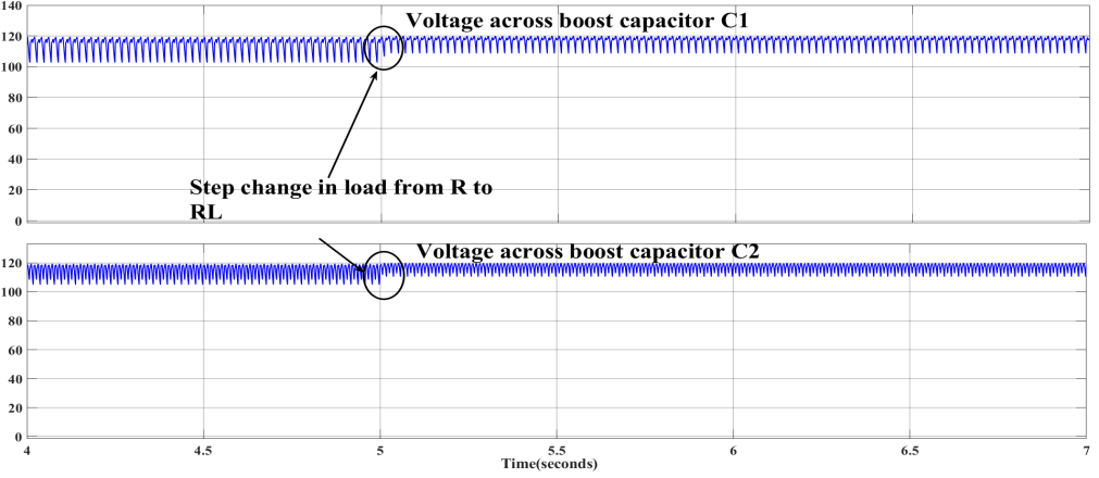
Figure 11. Voltage across Boost capacitors during dynamic change in load
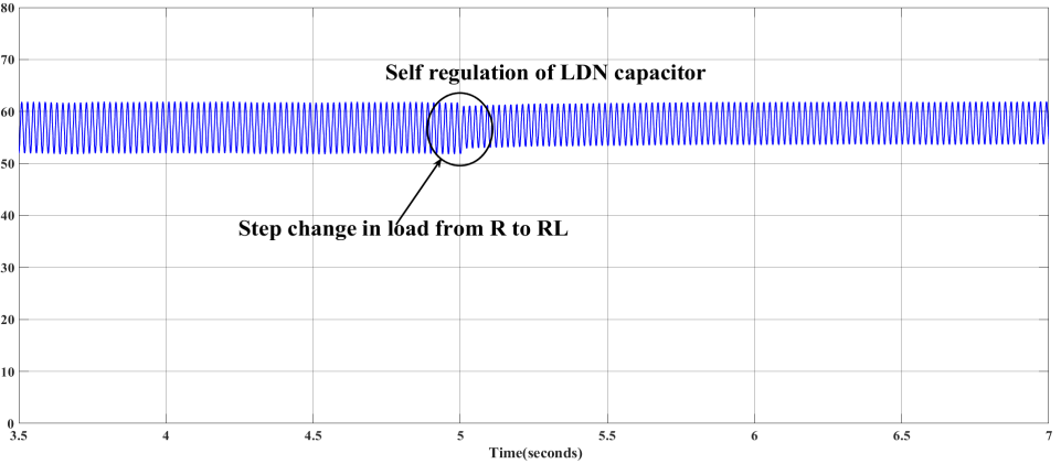
Figure 12. Voltage across LDN capacitor during dynamic change in load
The Figure 13 shows the load voltage and load current with a peak of magnitude of 300V and 4.9A respectively for the modulation of 0.8. Also, the voltage across the boost capacitor and LDN capacitor can be observed with reduced ripples as shown in the Figure 14 and Figure 15. Figure 16 shows the FFT analysis of the output voltage of the proposed topology. The THD of the output voltage is 10.85% for a modulation index of 0.95. The magnitude of the lower order harmonics is less than 1.5%, which simplifies the design of external filters. Furthermore, the load current THD is 0.81%, as shown in Figure 17, which is well below the limit prescribed by IEEE Std. 519-2022.
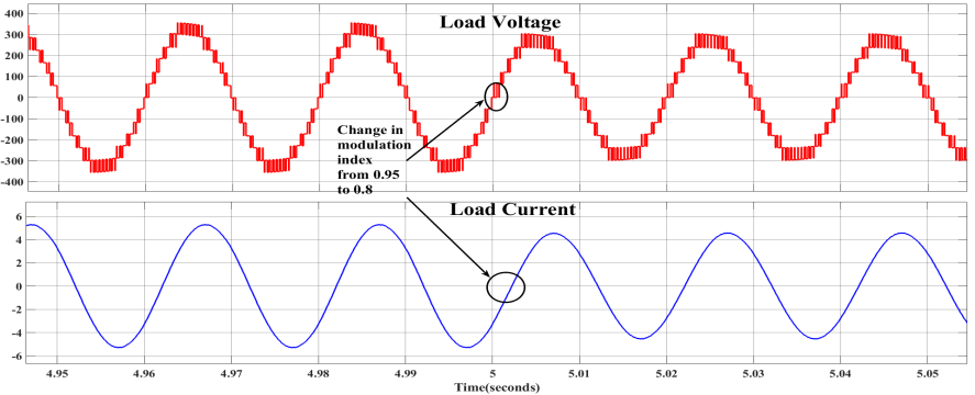
Figure 13. Load voltage and current during change in modulation index
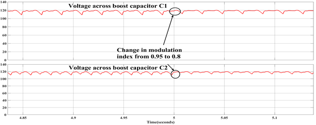
Figure 14. Voltage across Boost capacitors during change in modulation index
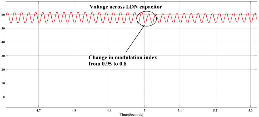
Figure. 15.Voltage across LDN capacitor during change in modulation index
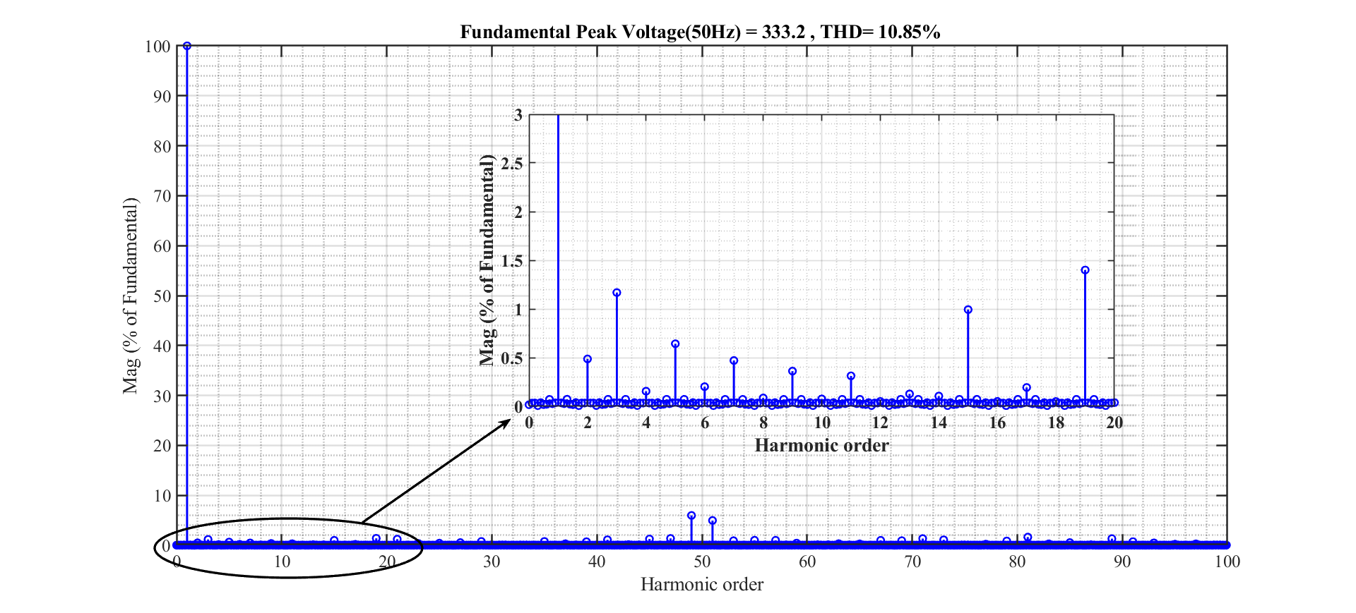
Figure 16. THD content of load voltage at steady state
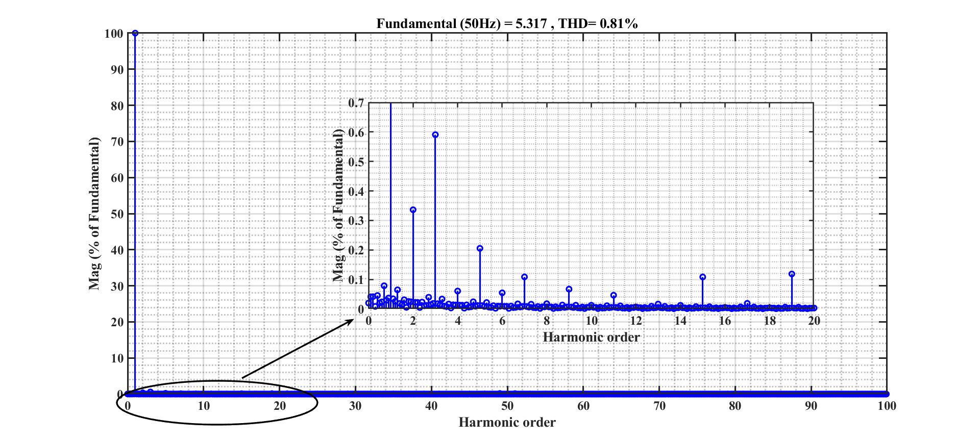
Figure 17. THD content of load current at steady state
- COMPARATIVE ASSESSMENT
The performance comparison is evaluated based on various components, including DC sources, switches, additional diodes, and capacitors to achieve different voltage levels and obtain the desired outcomes. These parameters are compared in Table 3. The sum of switches (NSW), diodes (ND), drivers (NGD), capacitors (NCAP), and total blocking voltage (TBV) of the converter multiplied by the number of DC (VDC) sources used constitutes the cost function of the inverter. This ratio is then multiplied by the number of voltage levels obtained. The value 1 is used in the computation to denote α, indicating that the input source voltage is equivalent to it. The expression for the cost function is articulated as follows,
| 
| (25) |
Where  is the number of DC sources used. MBV(*)- Maximum Blocking Voltage when the switch is in OFF condition; TBV(*)-Total Blocking Voltage;
  – Max number of conducting switches.
Table 3. Comparison of prop. Topology with similar existing topology
Ref | [33] | [34] | [35] | [36] | [37] | Proposed |
| 2 | 1 | 1 | 1 | 1 | 1 |

| 16 | 16 | 12 | 12 | 12 | 14 |

| 16 | 17 | 11 | 11 | 11 | 13 |

| 2 | 0 | 4 | 3 | 0 | 0 |

| 4 | 4 | 4 | 3 | 4 | 3 |
| 7 | 10 | 6 | 6 | 7 | 8 |
Gain | 3 | 3 | 3 | 3 | 1.5 | 3 |
TBV | 34 | 15.5 | 13 | 24 | 18 | 17 |
MBV | 6 | 2 | 2 | 2 | 2 | 2 |
CLF | 2.92 | 2.84 | 2.46 | 2.30 | 2.15 | 2.38 |
C.F | 10.76 | 4.03 | 3.4 | 4.07 | 3.46 | 3.6 |
The proposed circuit utilizes only one DC source to produce a 13-level output, which sets it apart from Multilevel Inverter (MLI) topology [33] that require multiple DC sources. This significantly reduces the number of voltage sources required, resulting in a more simplified and efficient design. Moreover, the proposed topology requires only 14 switches, which is second best among the recent topologies proposed in the literature. This reduction in the number of switches increases the reliability and decreases losses of the proposed topology. Additionally, the number of gate drivers required for this topology is only 13, whereas other topologies like [33] require 16 gate drivers respectively, further reducing the complexity of the proposed design.Another advantage of the proposed topology is that it does not require any additional diodes, which distinguishes it from other topologies like [33],[35][36], which require 2, 4 and 3 diodes respectively. This feature reduces the complexity and losses of the proposed design. The number of capacitors used in this topology is also minimal, only 3, compared to the other topologies like [33]-[35] and [37] which require 4 capacitors. In terms of blocking voltage of switches, the proposed topology has a Total Blocking Voltage (TBV) of 17, which is lower compared to topologies like [33],[36], and [37], which have TBVs of 34, 24, and 18 respectively. However, the Maximum Breakdown Voltage (MBV) of the proposed topology is only 2, which is less than the topology [33], which has an MBV of 6. Finally, the cost function calculated for the proposed topology is only 3.6, which is less than the cost functions of other topologieslike [33]-[34] and [36]. Eventhoughthe cost factor of [35] is less than the proposed inverter it has a higher CLF which makes it less reliable on account of higher component count. The voltage gain of [37] is 1.5 only. Thus, the proposed topology offers a simple, efficient, and cost-effective solution for applications where reliablity is important.
- CONCLUSION
This paper presents a thirteen-level multilevel inverter employing an LDN topology with a reduced number of devices, achieving an output voltage boosting factor of three. The paper provides a comprehensive description of the circuit topology, details the associated switching states, and presents the capacitance design methodology for a given load condition. The capacitors used in the proposed MLI are self-balanced, eliminating the need for auxiliary control methods or additional sensors, thus simplifying control complexity. The simulation results demonstrate the inherent boosting capability and operability of the proposed topology under various test scenarios,including changes in source, load, and modulation index. The proposed topology employs only three capacitors and eliminates the need for clamping diodes, resulting in a low cost factor and making it a superior alternative to existing topologies. The strong agreement between the theoretical analysis and the simulation results confirms the topology’s potential as a compact and efficient solution for renewable energy integration. Also, the future work will involve constructing a hardware prototype to validate the performance under real-world conditions.
ACKNOWLEDGEMENT
The authors wish to extend their gratitude to Mepco Schlenk Engineering College, Sivakasi, India, for providing the essential facilities needed to conduct this research.
REFERENCES
- S. Munawar, M. S. Iqbal, M. Adnan, M. Ali Akbar and A. Bermak, "Multilevel Inverters Design, Topologies, and Applications: Research Issues, Current, and Future Directions," in IEEE Access, vol. 12, pp. 149320-149350, 2024, https://doi.org/10.1109/ACCESS.2024.3472752.
- J. Rodriguez, Jih-Sheng Lai and Fang Zheng Peng, "Multilevel inverters: a survey of topologies, controls, and applications," in IEEE Transactions on Industrial Electronics, vol. 49, no. 4, pp. 724-738, 2002, https://doi.org/10.1109/TIE.2002.801052.
- A. Singh, V. Jately, P. Kala, Y. Yang and B. Azzopardi, "Advancements in Multilevel Inverters for Efficient Harnessing of Renewable Energy: A Comprehensive Review and Application Analysis," in IEEE Access, vol. 12, pp. 156939-156964, 2024, https://doi.org/10.1109/ACCESS.2024.3477501.
- S. Vaidya, K. Prasad, and J. Kilby, “The Role of Multilevel Inverters in Mitigating Harmonics and Improving Power Quality in Renewable-Powered Smart Grids: A Comprehensive Review,” Energies, vol. 18, no. 8, p. 2065, 2025, https://doi.org/10.3390/en18082065.
- A. Hren, M. Truntič, and F. Mihalič, “A Survey on the State-of-the-Art and Future Trends of Multilevel Inverters in BEVs,” Electronics, vol. 12, no. 13, p. 2993, 2023, https://doi.org/10.3390/electronics12132993.
- S. Alepuz et al., “A Survey on Capacitor Voltage Control in Neutral-Point-Clamped Multilevel Converters,” Electronics, vol. 11, no. 4, pp. 527–527, 2022, https://doi.org/10.3390/electronics11040527.
- S. Coday, N. Ellis, N. Stokowski and R. C. N. Pilawa-Podgurski, "Design and Implementation of a (Flying) Flying Capacitor Multilevel Converter," 2022 IEEE Applied Power Electronics Conference and Exposition (APEC), pp. 542-547, 2022, https://doi.org/10.1109/APEC43599.2022.9773635.
- M. Malinowski, K. Gopakumar, J. Rodriguez and M. A. Pérez, "A Survey on Cascaded Multilevel Inverters," in IEEE Transactions on Industrial Electronics, vol. 57, no. 7, pp. 2197-2206, 2010, https://doi.org/10.1109/TIE.2009.2030767.
- R. Bauwelz Gonzatti, Y. Li, M. Amirabadi, B. Lehman and F. Z. Peng, "An Overview of Converter Topologies and Their Derivations and Interrelationships," in IEEE Journal of Emerging and Selected Topics in Power Electronics, vol. 10, no. 6, pp. 6417-6429, 2022, https://doi.org/10.1109/JESTPE.2022.3181217.
- K. K. Gupta, A. Ranjan, P. Bhatnagar, L. K. Sahu and S. Jain, "Multilevel Inverter Topologies With Reduced Device Count: A Review," in IEEE Transactions on Power Electronics, vol. 31, no. 1, pp. 135-151, 2016, https://doi.org/10.1109/TPEL.2015.2405012.
- N. Prabaharan and K. Palanisamy, “A comprehensive review on reduced switch multilevel inverter topologies, modulation techniques and applications,” Renewable and Sustainable Energy Reviews, vol. 76, pp. 1248–1282, 2017, https://doi.org/10.1016/j.rser.2017.03.121.
- J. Venkataramanaiah, Y. Suresh, and A. K. Panda, “A review on symmetric, asymmetric, hybrid and single DC sources based multilevel inverter topologies,” Renewable and Sustainable Energy Reviews, vol. 76, pp. 788–812, 2017, https://doi.org/10.1016/j.rser.2017.03.066.
- M. Vijeh, M. Rezanejad, E. Samadaei and K. Bertilsson, "A General Review of Multilevel Inverters Based on Main Submodules: Structural Point of View," in IEEE Transactions on Power Electronics, vol. 34, no. 10, pp. 9479-9502, 2019, https://doi.org/10.1109/TPEL.2018.2890649.
- A. Salem, H. Van Khang, K. G. Robbersmyr, M. Norambuena and J. Rodriguez, "Voltage Source Multilevel Inverters With Reduced Device Count: Topological Review and Novel Comparative Factors," in IEEE Transactions on Power Electronics, vol. 36, no. 3, pp. 2720-2747, 2021, https://doi.org/10.1109/TPEL.2020.3011908.
- H. P. Vemuganti, D. Sreenivasarao, S. K. Ganjikunta, H. M. Suryawanshi and H. Abu-Rub, "A Survey on Reduced Switch Count Multilevel Inverters," in IEEE Open Journal of the Industrial Electronics Society, vol. 2, pp. 80-111, 2021, https://doi.org/10.1109/OJIES.2021.3050214.
- M. Trabelsi, H. Vahedi and H. Abu-Rub, "Review on Single-DC-Source Multilevel Inverters: Topologies, Challenges, Industrial Applications, and Recommendations," in IEEE Open Journal of the Industrial Electronics Society, vol. 2, pp. 112-127, 2021, https://doi.org/10.1109/OJIES.2021.3054666.
- M. Kumari, Marif Daula Siddique, A. Sarwar, M. Tariq, Saad Mekhilef, and A. Iqbal, “Recent trends and review on switched‐capacitor ‐based single‐stage boost multilevel inverter,” International Transactions on Electrical Energy Systems, vol. 31, no. 3, 2021, https://doi.org/10.1002/2050-7038.12730.
- M. S. W. Chan and K. T. Chau, "A New Switched-Capacitor Boost-Multilevel Inverter Using Partial Charging," in IEEE Transactions on Circuits and Systems II: Express Briefs, vol. 54, no. 12, pp. 1145-1149, 2007, https://doi.org/10.1109/TCSII.2007.905352.
- E. Babaei and S. S. Gowgani, "Hybrid Multilevel Inverter Using Switched Capacitor Units," in IEEE Transactions on Industrial Electronics, vol. 61, no. 9, pp. 4614-4621, 2014, https://doi.org/10.1109/TIE.2013.2290769.
- Y. Ye, K. W. E. Cheng, J. Liu and K. Ding, "A Step-Up Switched-Capacitor Multilevel Inverter With Self-Voltage Balancing," in IEEE Transactions on Industrial Electronics, vol. 61, no. 12, pp. 6672-6680, 2014, https://doi.org/10.1109/TIE.2014.2314052.
- Y. Hinago and H. Koizumi, "A Switched-Capacitor Inverter Using Series/Parallel Conversion With Inductive Load," in IEEE Transactions on Industrial Electronics, vol. 59, no. 2, pp. 878-887, 2012, https://doi.org/10.1109/TIE.2011.2158768.
- R. Barzegarkhoo, Y. P. Siwakoti, R. P. Aguilera, M. N. H. Khan, S. S. Lee and F. Blaabjerg, "A Novel Dual-Mode Switched-Capacitor Five-Level Inverter With Common-Ground Transformerless Concept," in IEEE Transactions on Power Electronics, vol. 36, no. 12, pp. 13740-13753, 2021, https://doi.org/10.1109/TPEL.2021.3074517.
- M. Saeedian, M. E. Adabi, S. M. Hosseini, J. Adabi and E. Pouresmaeil, "A Novel Step-Up Single Source Multilevel Inverter: Topology, Operating Principle, and Modulation," in IEEE Transactions on Power Electronics, vol. 34, no. 4, pp. 3269-3282, 2019, https://doi.org/10.1109/TPEL.2018.2848359.
- R. Barzegarkhoo, M. Moradzadeh, E. Zamiri, H. Madadi Kojabadi and F. Blaabjerg, "A New Boost Switched-Capacitor Multilevel Converter With Reduced Circuit Devices," in IEEE Transactions on Power Electronics, vol. 33, no. 8, pp. 6738-6754, 2018, https://doi.org/10.1109/TPEL.2017.2751419.
- W. Peng, Q. Ni, X. Qiu and Y. Ye, "Seven-Level Inverter With Self-Balanced Switched-Capacitor and Its Cascaded Extension," in IEEE Transactions on Power Electronics, vol. 34, no. 12, pp. 11889-11896, 2019, https://doi.org/10.1109/TPEL.2019.2904754.
- A. Taghvaie, J. Adabi and M. Rezanejad, "A Self-Balanced Step-Up Multilevel Inverter Based on Switched-Capacitor Structure," in IEEE Transactions on Power Electronics, vol. 33, no. 1, pp. 199-209, 2018, https://doi.org/10.1109/TPEL.2017.2669377.
- R. Barzegarkhoo, H. M. Kojabadi, E. Zamiry, N. Vosoughi and L. Chang, "Generalized Structure for a Single Phase Switched-Capacitor Multilevel Inverter Using a New Multiple DC Link Producer With Reduced Number of Switches," in IEEE Transactions on Power Electronics, vol. 31, no. 8, pp. 5604-5617, 2016, https://doi.org/10.1109/TPEL.2015.2492555.
- B. Ngo, M. Nguyen, J. Kim, and F. Zare, “Single‐phase multilevel inverter based on switched‐capacitor structure,” IET Power Electronics, vol. 11, no. 11, pp. 1858–1865, 2018, https://doi.org/10.1049/iet-pel.2017.0857.
- J. Liu, W. Lin, J. Wu and J. Zeng, "A Novel Nine-Level Quadruple Boost Inverter With Inductive-Load Ability," in IEEE Transactions on Power Electronics, vol. 34, no. 5, pp. 4014-4018, 2019, https://doi.org/10.1109/TPEL.2018.2873188.
- N. Sandeep, J. S. M. Ali, U. R. Yaragatti and K. Vijayakumar, "Switched-Capacitor-Based Quadruple-Boost Nine-Level Inverter," in IEEE Transactions on Power Electronics, vol. 34, no. 8, pp. 7147-7150, 2019, https://doi.org/10.1109/TPEL.2019.2898225.
- M. D. Siddique et al., “Switched‐capacitor‐based boost multilevel inverter topology with higher voltage gain,” Iet Power Electronics, vol. 13, no. 14, pp. 3209–3212, 2020, https://doi.org/10.1049/iet-pel.2020.0446.
- S. S. Lee, "Single-Stage Switched-Capacitor Module (S3CM) Topology for Cascaded Multilevel Inverter," in IEEE Transactions on Power Electronics, vol. 33, no. 10, pp. 8204-8207, 2018, https://doi.org/10.1109/TPEL.2018.2805685.
- T. Roy, P. K. Sadhu, and A. Dasgupta, “Cross-Switched Multilevel Inverter Using Novel Switched Capacitor Converters,” IEEE Transactions on Industrial Electronics, vol. 66, no. 11, pp. 8521–8532, 2019, https://doi.org/10.1109/tie.2018.2889632.
- W. Lin, J. Zeng, J. Liu, Z. Yan, and R. Hu, “Generalized Symmetrical Step-Up Multilevel Inverter Using Crisscross Capacitor Units,” IEEE Transactions on Industrial Electronics, vol. 67, no. 9, pp. 7439–7450, 2019, https://doi.org/10.1109/tie.2019.2942554.
- K. P. Panda, P. R. Bana, and G. Panda, “A Reduced Device Count Single DC Hybrid Switched-Capacitor Self-Balanced Inverter,” IEEE Transactions on Circuits & Systems II Express Briefs, vol. 68, no. 3, pp. 978–982, 2020, https://doi.org/10.1109/tcsii.2020.3018333.
- S. Islam, M. D. Siddique, A. Iqbal, S. Mekhilef, and M. Al-Hitmi, “A Switched Capacitor-Based 13-Level Inverter With Reduced Switch Count,” IEEE Transactions on Industry Applications, vol. 58, no. 6, pp. 7373–7383, 2022, https://doi.org/10.1109/tia.2022.3191302.
- J. Zeng, W. Lin, D. Cen and J. Liu, "Novel K-Type Multilevel Inverter With Reduced Components and Self-Balance," in IEEE Journal of Emerging and Selected Topics in Power Electronics, vol. 8, no. 4, pp. 4343-4354, 2020, https://doi.org/10.1109/jestpe.2019.2939562.
- Y. Ye, S. Chen, X. Wang, and K.-W. E. Cheng, “Self-Balanced 13-Level Inverter Based on Switched Capacitor and Hybrid PWM Algorithm,” IEEE Transactions on Industrial Electronics, vol. 68, no. 6, pp. 4827–4837, 2020, https://doi.org/10.1109/tie.2020.2989716.
- N. Sandeep, “A 13-Level Switched-Capacitor-Based Boosting Inverter,” IEEE Transactions on Circuits and Systems II: Express Briefs, vol. 68, no. 3, pp. 998–1002, 2021, https://doi.org/10.1109/tcsii.2020.3017338.
- N. S. Hasan, N. Rosmin, D. A. A. Osman, and A. H. Musta’amal, “Reviews on multilevel converter and modulation techniques,” Renewable and Sustainable Energy Reviews, vol. 80, pp. 163–174, 2017, https://doi.org/10.1016/j.rser.2017.05.163.
- A. Poorfakhraei, M. Narimani and A. Emadi, "A Review of Modulation and Control Techniques for Multilevel Inverters in Traction Applications," in IEEE Access, vol. 9, pp. 24187-24204, 2021, https://doi.org/10.1109/ACCESS.2021.3056612.
- Satılmış Ürgün, Halil Yiğit, and Seyedali Mirjalili, “Investigation of Recent Metaheuristics Based Selective Harmonic Elimination Problem for Different Levels of Multilevel Inverters,” Electronics, vol. 12, no. 4, pp. 1058–1058, 2023, https://doi.org/10.3390/electronics12041058.
- N. A. Rahim, K. Chaniago and J. Selvaraj, "Single-Phase Seven-Level Grid-Connected Inverter for Photovoltaic System," in IEEE Transactions on Industrial Electronics, vol. 58, no. 6, pp. 2435-2443, 2011, https://doi.org/10.1109/TIE.2010.2064278.
- S. K. Chattopadhyay and C. Chakraborty, "A New Multilevel Inverter Topology With Self-Balancing Level Doubling Network," in IEEE Transactions on Industrial Electronics, vol. 61, no. 9, pp. 4622-4631, 2014, https://doi.org/10.1109/TIE.2013.2290751.
AUTHOR BIOGRAPHY

| Sakthisudhursun Balakrishnan has been with Mepco Schlenk Engineering College, Sivakasi since 2014, where he is currently working as Assistant Professor (Selection Grade). He received his B.E., and M.Tech. from PSG College of Technology, Coimbatore and Visvesvaraya National Institute of Technology, Nagpur, India respectively. He completed his Ph.D., at Anna University in the year 2024. His research interests include Multilevel Inverters, SVPWM, multiphase multilevel drives, and DC–DC converters for distributed generation.He can be contacted at email: sakthisudhursun@gmail.com, bss@mepcoeng.ac.in |
|
|

| Muralidharan Srinivasan the B.E. degree in Electrical Engineering from Madurai Kamaraj University, Madurai, India, the M.S. degree in Software Systems from the Birla Institute of Technology and Science, Pilani, Rajasthan, India, and the Ph.D. degree from SASTRA University, Thanjavur, Tamil Nadu, India, in 1994, 1997, and 2009, respectively. He is serving as a Senior Professor in the Department of Electrical and Electronics Engineering, MEPCO Schlenk Engineering College, Sivakasi, Tamil Nadu. He has published several technical papers in refereed international journals and international conferences. His research interests include special electrical machines and soft computing applications in electrical power system. He can be contacted at email: smurali@mepcoeng.ac.in |
|
|

| Sundaramahalingam Subramaniam graduated in Electrical and Electronics Engineering from SSN College of Engineering, Chennai in 2010. In 2012, he received Master of Engineering in High Voltage Engineering from the College of Engineering Guindy, Anna University, India. He completed his Ph.D in the field of High Voltage Engineering under Anna University, Chennai, India in 2025. He had 12.5 years of teaching experience and currently he is working as an Assistant Professor (Selection Grade) in the Department of Electrical Engineering at Mepco Schlenk Engineering College (Autonomous), Sivakasi, India. His research activities are focused on Finite Element Analysis of Electrical Equipments, Control of Electric Machines and Drives. He can be contacted at email: sundar.eee@mepcoeng.ac.in |
|
|

| Vanaja Narayanaswamy obtained her under graduation in Electrical and Electronics Engineering from Mepco Schlenk Engineering College, Sivakasi in the year 2010, post graduation in Power Electronics and Drives from Mepco Schlenk Engineering College, Sivakasi in the year 2014 and Ph.D from Anna University, Chennai in the year 2025. She is working in Mepco Schlenk Engineering College, Sivakasi since 2010 where currently she is working as Assistant Professor (Selection Grade). Her area of interest are power quality enhancement of grid-tied inverter and soft computing techniques. Email: nvanaja@mepcoeng.ac.in |
Sakthisudhursun Balakrishnan (A Self-Balancing 13-Level Single-Phase Triple Gain Inverter)